Loading...
News Article

Fraunhofer IMS opens up photonic integration capabilities

News
Invites participation in engineering runs on its SiN-based PIC platform

Fraunhofer IMS is opening up its photonic integration capabilities to participants who would like to engage in engineering runs (starting Q1 2025) to create their own PIC designs in a high-quality clean room.

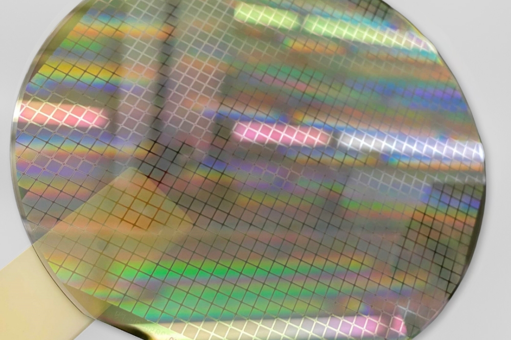
The Fraunhofer IMS SiN-based photonic platform (built on 200 mm wafers) supports low-loss, broad-wavelength applications. It offers the possibility of novel quasi-monolithic integration with a wide range of waveguide materials, including, for example, SiN, tantalum pentoxide (Ta2O5), covering visible to mid-infrared wavelengths from 370 nm to 3 µm. Current photonic components include couplers, waveguides, and interferometers, with the option for custom designs.

Fraunhofer IMS says it offers strong support for technology, device, and circuit simulations, considering packaging and system-level needs.

With expertise in microelectronics, micro-electromechanical systems (MEMS), and photonics, Fraunhofer IMS focuses on post-CMOS integration of PICs for smart sensor systems. This includes working with external foundry wafers for applications in optical computing, biosensors, and on-chip quantum photonics.

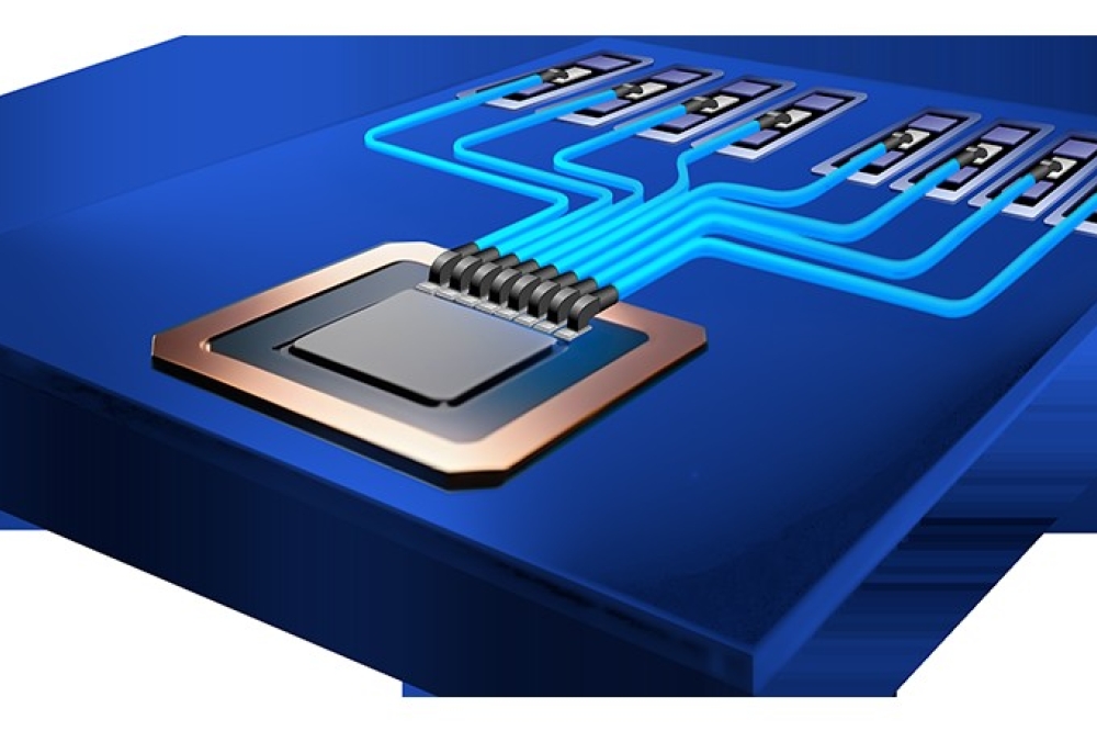
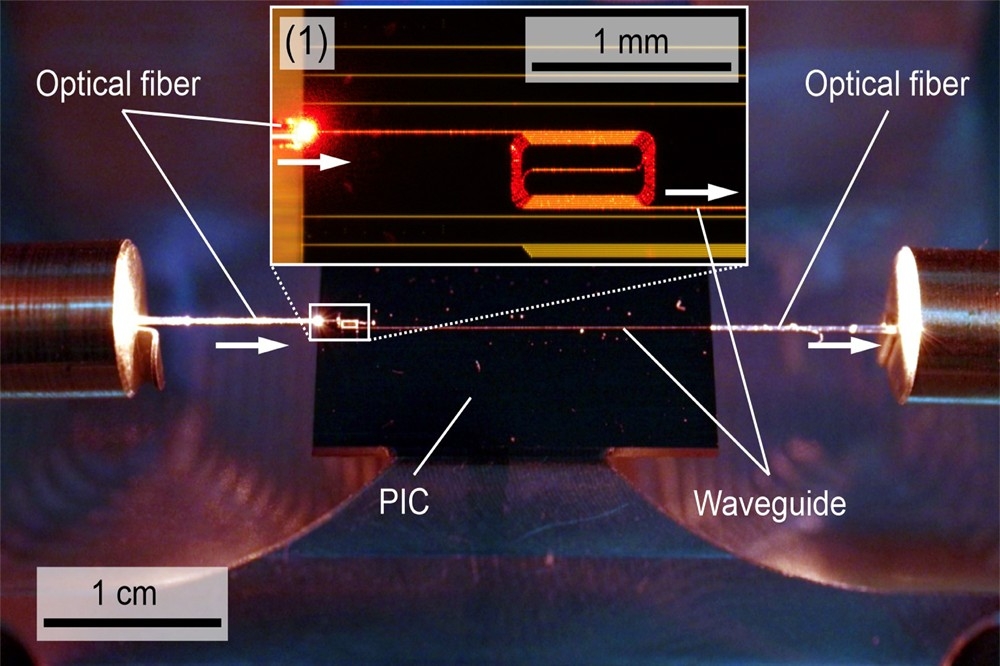
Photograph above shows edge coupling into and out of a cutback structure using 633 nm light. Inset (1): Microscope image of the cutback structure and coupling area.

SPONSOR MESSAGE

Secure Your Hydrogen Supply

A study supply of high-purity hydrogen is critical to semiconductor fabrication. Supply chain interruptions are challenging manufacturers, leading to production slowdowns and stoppages. On-site hydrogen generation offers a scalable alternative for new and existing fabs, freeing the operator from dependence on delivered gas.

Plant managers understand the critical role that hydrogen plays in semiconductor fabrication. That important job includes crystal growth, carrier gas, wafer annealing, and in the emerging Extreme UV Lithography (EUV) that will enable new generations of devices. As the vast need for semiconductors grows across all sectors of world economies, so does the need for high-purity hydrogen.

Take control with Nel on-site hydrogen generation.

Read more
×
Search the news archive

To close this popup you can press escape or click the close icon.
Logo
x
Logo
×
Register - Step 1

You may choose to subscribe to the Compound Semiconductor Magazine, the Compound Semiconductor Newsletter, or both. You may also request additional information if required, before submitting your application.


Please subscribe me to:


You chose the industry type of "Other"

Please enter the industry that you work in:
 
x
Adblocker Detected
Please consider unblocking adverts on this website