Superior sealing

Greene Tweed’s portfolio of precision seals offers tremendous support to empower the growth of the compound semiconductor industry.
BY PRAGATI VERMA AND THYAG SADASIWAN FROM GREENE TWEED
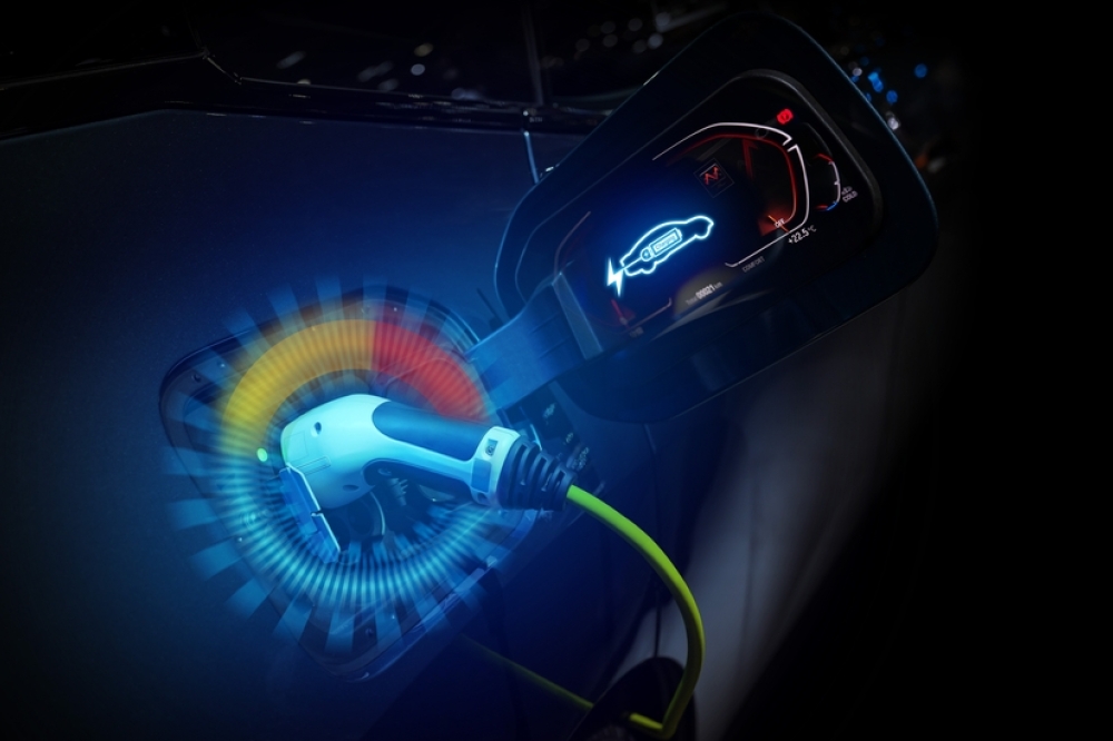
From ultra-fast communication and electric vehicles to energy applications and artificial intelligence, today’s most innovative technologies rely on compound semiconductors. Excelling where silicon falls short, the unique properties of these chips support the innovation that’s required for tomorrow’s breakthroughs.
Given the growing demand for compound semiconductor technologies, it’s of little surprise that this industry is generating substantial and growing sales. While well-established devices – such as LEDs that serve in general lighting and GaAs-based power amplifiers that are a key ingredient in mobile phones – no longer enjoy rapidly rising revenues, sales are growing fast in other sectors. The most notable of these is that of SiC power electronics, now deployed in automotive, industrial, energy, and rail applications. According to semiconductor market research analyst Yole Group, the SiC device market will increase in value to $10 billion over the next five years, with SiC substrate and epiwafer shipments growing to over 3 million units.

When it can’t fail
Driven by opportunities to grow their revenues, many makers of compound semiconductor devices are pursuing capacity expansion plans. Their investments will take many forms, from tools for epitaxial growth and metrology to securing a steady supply of a number of inconspicuous yet indispensable components.
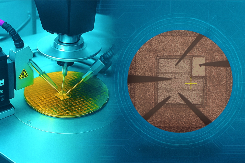
The latter includes products that play a critical role in the manufacture of compound semiconductors, such as the patented Chemraz sealing technology developed by our company, Greene Tweed.
Well known for having have a strong pedigree in this area, we are a global leader in perfluoroelastomer (FFKM) Chemraz sealing solutions. It’s an enviable position that we are not taking for granted, as we continue to lead the way with multi-million-dollar investments in facilities, alongside the launch of several new products and manufacturing automation technologies.
Several prominent chipmakers depend on our Chemraz seals. Using them for the production of their most powerful chips, they view second-best seals as not good enough for challenging manufacturing environments.
Demand for our products is growing as chipmakers turn to our Chemraz O-rings and sealing solutions for more demanding processes, where they are able to prevent contamination while withstanding aggressive chemicals and extremely high temperatures. When operating in the world’s harshest semiconductor manufacturing applications, our products combine a tremendous level of performance with exceptional reliability.
Another factor that makes our Chemraz seals indispensable relates to the increasing need for ultraclean processing in manufacturing applications. As the first sealing solutions company to use cleanroom manufacturing in the US, we fully understand the significance of ultraclean operations in the semiconductor industry. We have devoted much effort to ensure that our seals control particle excursions that threaten contamination, while they increase uptime and boost wafer yield.
Balancing performance and costs
Greene Tweed understands that not every semiconductor application needs a Chemraz sealing solution. That’s where our Fusion FKM (fluoroelastomer) products come in. They are field-tested in extreme temperatures, high pressures, corrosive chemicals, and volatile fluids.
The Fusion 707 has been specifically developed for flat panel display CVD and dry plasma etch equipment, where seal reliability and minimal contamination are essential. The 707 family of seals provides excellent chemical resistance and withstands various aggressive chemicals. Related to them is the Fusion 706 – it is ideal for a range of plasma equipment applications, from etch and plasma-enhanced CVD to plasma ashing applications, as well as those that must accommodate low sealing force materials, such as bonded slit valve gates.
Introduced earlier this year is the Fusion F07. This sealing solution is crafted to withstand common etch and CVD oxygen/fluorine-based gases in semiconductor processing sub-fab lines. The F07 handles continuous operating temperatures up to 180 °C and has a minimum expected lifetime of six months. These figures are both better than those for standard FKM seals serving in the same applications. What’s more, the F07 offers a lower cost of operations than premium FFKM materials.
That’s not all. Greene Tweed’s products help trim the costs of upgrading to larger wafers, such as a move from 150 mm to 200 mm. Note that the manufacture of compound semiconductor, such as SiC, is more expensive, due to the high cost of material, as well as more complex manufacturing processes and lower production yields.
Many companies are trying to reduce the costs of switching to larger wafers by acquiring older tools and modifying and retrofitting them with software upgrades, so that they can work with the likes of SiC, or other compound materials. As some of these tools come with older and obsolete components, we are offering upgrade seal kits to improve the capabilities of older refurbished tools, a more prudent alternative to making massive investments in entirely new equipment. By upgrading tools so that they can incorporate the latest high-performance sealing solutions required to prevent contamination and maintain a cleanroom environment, compound semiconductor manufacturers can increase throughput and yield, critical to meeting the surge in demand while optimising profitability.
Scaling up to provide chipmakers with the products that they will need during the anticipated boom is far from trivial. But the recent industry-wide supply crunch gripping the FFKM materials, which has coincided with a global surge in demand for chips, has given us valuable insights into how to meet the burgeoning demand while minimising the impact of possible disruptions.
Building on these insights, we are rolling out six major initiatives to ensure that we can promptly deliver high-performing sealing solutions, as customer needs evolve to meet the growing demand for semiconductors. These six initiatives, which we go on to discuss in detail, are: a new manufacturing facility in Korea; new innovations, designed for harsh conditions and expansion; the introduction of next-generation manufacturing to accelerate growth; the use of secured resources; fortification of supply chain resiliency; and ensuring that we are ready for the new tools that chipmakers will invest in.
A new facility in Korea
We are making significant investments to expand our global manufacturing capacity and capabilities within the semiconductor market. This initiative is exemplified by our construction of a new 6,500 m2 facility in Ochang, Cheongju-si, Chungcheongbuk-do, South Korea. Our new factory is equipped with end-to-end manufacturing process capabilities – from initial extrusion of raw materials to warehousing finished products. We have already started producing samples, and later this year we will transition to commercial production.
Featuring cleanroom space to maintain a pristine environment vital for components supporting chip fabrication, our new facility in South Korea will initially focus on our flagship Chemraz product line.
As well as increasing global capacity, this new facility for producing Chemraz products is underscoring our commitment to supporting customers based in South Korea and the surrounding region, including notable semiconductor leaders. This facility, which is creating a healthier global supply chain, will help us shorten lead times, build stronger co-development strategies with key customers, and enhance business continuity plans.

Aside from advanced manufacturing technology, our state-of-the-art plant in South Korea is equipped with solar panels and greywater recycling facilities to mitigate the environmental impact.
What’s more, our new facility is designed with scalability in mind. It offers ample room for growth, enabling us to expand our production capabilities as demand increases. Over the next few years, we will be implementing a phased rollout of new production lines. This effort will begin by increasing capacity and adding automated equipment to enhance our production processes and reduce our lead times. Beyond that, we will be focusing on expansion, including an additional cleanroom, and integrating cutting-edge manufacturing technologies and processes.
Our long-term strategy is to ensure that we remain agile and responsive to our customers’ evolving needs, while the demand for semiconductors grows over the remainder of this decade and beyond.
Outperforming in harsh conditions
As a global leader in FFKM seals, Greene Tweed knows that our Chemraz seals are critical for the most advanced semiconductor fabrication processes. To support our customers’ growing needs, we have introduced two new high-performing, price-competitive products – the Chemraz G38 and G57.
This pair of products are designed to meet the evolving needs of various plasma applications, while being incredibly price competitive and delivered with world-class lead times. By expanding our line-up in this way, we are demonstrating our commitment to continuously innovating and responding to the demands of the market and ensuring that our customers have the best solutions at their disposal.
Custom-engineered to meet the demands of aggressive dry plasma systems, our Chemraz G57 technology provides improved plasma resistance and minimises contamination, resulting in less downtime and higher wafer processing yields in both static and dynamic oxide etch wafer-processing applications. This product has excellent chemical resistance and withstands temperatures up to 300 °C, making it ideal for several applications, including endpoint windows, window seals, slit valve seals, bell jar seals, isolator valve seals, chamber seals, valve seals, lid seals, KF fitting seals, and gas inlet seals.
Meanwhile, the Chemraz G38 is targeting high-density plasma systems, where seal reliability and minimal contamination are essential. The G38 has excellent chemical compatibility and is capable of withstanding a variety of aggressive chemicals.
Recommended for bonded gate seals and chamber seals, this product delivers exceptional value in a number of applications, including deposition, remote plasma cleans, oxidation, diffusion, ion implant, implant anneal, and rapid thermal processing.
Our development of new technologies continues at pace, and we have another Chemraz sealing solution ready to roll out in the next 6-12 months. Helping to encourage us in this endeavour is the adoption of our existing sealing solutions, including Chemraz and Fusion F07 FKM, in semiconductor fabs being built all around the world.

Next-gen manufacturing
We are committing significant resources to automating manufacturing processes, as this enables us to scale capacity and quickly meet the growing needs of our evolving semiconductor customers. By supplementing core manufacturing processes with robotics and digital solutions, we are supporting production floor employees to eliminate process bottlenecks and trim lead times.
Our largest investments are associated with high-impact process steps, such as compression moulding, inspection, and packaging. The reasoning behind this is that it maximises efficiency and productivity gains. For compression moulding, operators are currently responsible for moving and servicing moulds between every cycle. However, we are moving towards an automated approach, using a 6-axis robot to move moulds. This will allow the operator to focus only on value-added activities and service more moulding presses. Similarly, for current packaging operations, our operators are responsible for bagging and labelling parts individually – this is slow and tedious. Due to this, we are introducing an automated solution, involving multiple robots and an automatic bagging machine, as this will increase throughput and standardise bagging quality.
We are also building and utilising digital twins. It’s a move that will allow us to proactively evaluate new innovative technologies and discover how to best introduce them into existing manufacturing facilities.
By turning to these technologies and dedicated technical resources, we are transforming our production lines. They are becoming more adaptable, and they are allowing us to scale up quickly to meet our customers’ needs without compromising on excellence.
Secured resources
Expanding our manufacturing capacity is just one of the prongs of our multi-faceted strategy that is laying the foundations for supporting a strong upturn in the market. To ensure world-class lead times, we have secured a reliable supply of raw materials from multiple suppliers. With these partners, we are well-positioned to cater for an anticipated ramp in chip production over the next two years.
While running four factories with balanced workloads, we have significantly increased our workforce to stabilise the production process, in conjunction with bolstering our manufacturing capabilities by introducing new equipment in our plants in Korea, Taiwan and Selma. As well as keep pace with growth, these strategic moves will enhance our production capabilities, minimise delays, and accelerate delivery times.
Fortified supply chain resiliency
As we work to secure a steady supply of raw materials, we are proactively reducing our reliance on a single vendor or market. Here’s why: The industry-wide FFKM supply crunch, which occurred during the pandemic-led surge in demand for semiconductors, has taught us the importance of diversifying and strengthening our supply chain. That’s why we have carefully selected multiple sources of raw materials, located in separate regions.
Proactively identifying and mitigating many potential risks, ranging from those that are geo-political to those associated with regulatory matters and climate change events, has enabled us to build comprehensive supply chain resiliency, as well as a business continuity plan that we share with customers to ensure transparency. By securing raw materials and building supply chain resiliency, our customers benefit from reduced downtime, helping them to meet the incredibly tight production schedules they face during fast-increasing demand when markets are booming. This is critical in many sectors within the semiconductor industry, where missing a time-to-market window threatens to slash sales.
Preparing for new tools
Our innovation in sealing solutions supports the unique needs of the compound semiconductor market, as well as the latest technology inflections in the silicon industry.We work with OEMs across these markets as they upgrade their tools to serve their customer base. Whether it’s the latest innovations in etch or in deposition, we are taking proactive steps to keep up with market demand
and growth.
For example, our bonded slit valves, lip seals, seals for electroplating solutions, vacuum line solutions, cryogenic seals, and many other sealing solutions are continuing to be widely adopted by equipment makers, creating value and yield enhancement for both silicon and compound semiconductor fabs. Most recently, Xyfluor materials have been qualified for use in electrostatic chucks that can operate at temperatures as low as -40 °C.
Ready for growth
Building cutting-edge compound semiconductor chips is a challenging, cost-intensive process that hinges on small yet essential components, such as our sealing solutions. Working closely with our customers and partners, we are ready to address the burgeoning need for sealing solutions from chipmakers, thereby ensuring the scalability and sustainability of their operations for the rest of this decade and beyond.