Revolutionising RF oscillators with GaN
GaN IMPATT diodes can enable compact and efficient solid-state
oscillators that deliver higher powers in the millimetre-wave and beyond.
BY ZHENGLIANG BIAN AND SRABANTI CHOWDHURY FROM STANFORD UNIVERSITY
To advance modern RF applications, much effort is directed at realising a higher RF power within a compact form factor. There are a number of solid-state devices that can do this, but the most compelling for efficient high-RF-power generation is the impact ionisation avalanche transit time (IMPATT) diode. This form of diode, which is capable of delivering an exceptionally high output power from a few gigahertz to hundreds of gigahertz, can replace elaborate multiplier and amplifier chains.
While you may not be that familiar with the IMPATT diode, it is certainly not a new device. Its inception dates back to 1958, when W.T. Read, working at Bell Laboratories, proposed a simple p-n structure that consists of a narrow avalanche carrier multiplication region followed by a drift region (see Figure 1). Read theorised that a 180° phase shift occurs with the applied voltage, due to the combination of the time delay associated with avalanche multiplication and the transit time of the injected carriers traveling through the drift region. This phase shift gives rise to a negative resistance that contributes to RF power generation.

Figure 1. (a) The design of the Read-type IMPATT diode. (b) Voltage transient at the cathode for an IMPATT under oscillation. (c) A carrier generation waveform in the avalanche region. (d) The induced terminal current for an IMPATT under oscillation.
In 1965 the first IMPATT oscillation was observed, in a device made from silicon. This triumph laid the groundwork for significant advances in IMPATT technology over the following decades, including the deployment of this device in satellite communications and radar systems. Today, a single commercial IMPATT diode, mostly realised with silicon technology, is capable of delivering 400 mW under continuous-wave mode and 20 W under pulsed-mode operation at 94 GHz.
Embracing GaN’s benefit
Despite the success of the silicon IMPATT diode, the quest remains to develop higher-performance devices that draw on current RF technology. Throughout the evolution of the compound semiconductor industry, new materials have played a pivotal role in pushing the boundaries of device performance. It is a state-of-affairs that is no different with the IMPATT diode, where GaN in particularly is reviving interest in this device.
Due to its tendency to be deployed as an oscillator, the primary performance metric for the IMPATT diode is its power-frequency trade-off. Analysis reveals that both the output power and the oscillation frequency of an IMPATT diode are mainly determined by the critical field and the saturation velocity in the base material. The output power of the diode is proportional to both the square of the critical field and the square of the saturation velocity, and inversely proportional to the square of the frequency. Based on these relationships, GaN clearly has the upper hand over silicon (see Figure 2), thanks to a critical field that is 10 times higher, and twice the saturation velocity. Combining these attributes indicates that the GaN IMPATT diode has a 400 times higher power capability than its silicon counterpart at a given frequency.

Figure 2. Material properties for various candidate
materials for IMPATT oscillators, and a power-frequency benchmark plot.
Another promise of the GaN-based IMPATT diode is that it is projected to have a much higher cut-off frequency – it is in the terahertz range – due to its shorter avalanche response time. This makes the GaN IMPATT diode an attractive solid-state terahertz source that could enable various novel applications, such as high-resolution imaging through opaque materials for medical diagnosis and security screening, and extreme wideband wireless communications.
Current status
Unfortunately, engineers have struggled to convert the tremendous promise of the GaN IMPATT diode into a high-performance device. But the good news is that this situation is starting to change. Helping to facilitate this are improvements in producing low-defect-density bulk GaN substrates, high-quality epitaxy growth, and effective edge terminations – all these advances are crucial to routinely realising avalanche in GaN p-n diodes.
Initial efforts with GaN involved embedding a p-n diode in a series resonate circuit and observing an 800 MHz oscillation. This weak, low-frequency oscillation has been attributed to limitations associated with significant device self-heating and low-quality oscillation circuitry. Improvements were wrought by placing the diode on a copper heat sink and testing it under pulsed mode in a waveguide resonate cavity. This recent work, involving a GaN IMPATT diode, enabled a peak power of 30 dBm to be extracted up to 21 GHz.
While these results are encouraging, as well as failing to unlock GaN’s potential, they don’t even exceed the performance of their silicon counterparts. Why is this? It’s because GaN is held back by immature fabrication techniques. In sharp contrast, the performance of silicon IMPATT diodes draws on refinements in device fabrication and packaging procedures that result in a robust avalanche, minimised series resistance, and adequate heat removal – all are crucial.
With GaN, the fabrication processes for excelling on these fronts are still immature. To address these weaknesses, our team at Stanford University is pursuing the following pair of goals: the development of a substrate thinning process that results in 20 µm-thick wafers that do not lead to degradation of avalanche in the fabricated diodes; and flip-chip packaging to a type IIA single crystalline diamond heat sink, to ensure enhanced heat dissipation.

Figure 3. The process flow for fabricating our GaN IMPATT diodes, and a photo of a packaged diode.
Innovative fabrication processes
Vital to our success is the introduction of a new process flow, involving diode fabrication, substrate thinning and packaging (this is illustrated in Figure 3). We begin by growing our desired epilayers by MOCVD on native bulk GaN substrates, and then incorporate a 5° bevelled mesa etch to mitigate field crowding around the mesa corner and enable avalanche. Here, our key technology is the introduction of a thinning and packaging process that does not compromise the avalanche in the diodes.
Note that a thinning process is critical to achieving high-frequency IMPATT diodes. For those made from silicon and operating in the W-band, a thickness of less than 10 µm is employed to minimise the series resistance coming from the substrate. A number of methods have been reported for realising a thin film of GaN, such as laser lift-off, nickel stressor spalling, and photoelectrochemical etching. However, none of these methods has been shown to enable avalanche compatibility.
We have overcome this obstacle with a two-step thinning process. This begins with mechanical lapping, to thin the GaN wafer down to around 150 µm, before we turn to a more gentle etching process for additional thinning. By adopting this hybrid approach, we avoid the threat of shattering the GaN wafer during the thinning process.
Validation of this process has come from examining the current-voltage characteristics of our diodes after thinning (see Figure 4). Plots reveal that the breakdown voltage does not change for our diodes on a thinned 20 µm-thick GaN wafer, and the leakage current remains minimal. The results also show a positive temperature coefficient in the breakdown voltage, confirming preservation of avalanche behaviour.

Figure 4. Breakdown characteristics comparison between diodes on (a) an un-thinned 400 mm-thick wafer and (b) a 20 mm-thick wafer after thinning.
One of the benefits of thinning our substrates from 400 µm to 20 µm is a trimming of the total on-resistance by 43 percent, thanks to elimination of series resistance originating from the substrate. However, there is an increase in contact resistance, which indicates that the formation of the backside contact after the thinning process demands additional improvement to maximise the benefit of substrate thinning.
It is important to properly package our IMPATT diodes before they are embedded in an oscillation circuit. For this task we select a flip-chip-style ceramic pill package, as shown in Figure 5. In this configuration, a heat sink is directly bonded to the anode to quickly remove the heat that’s generated around the p-n junction.
For this packaging process, we begin by bonding the GaN IMPATT diode to a diamond heat sink by thermal compression, and then solder quartz rings, which serve as a mechanical support and electrical isolators. Formation of the cathode follows, realised by connecting the backside of the diode to the top conductive seal with gold ribbons. We have optimised this packaging process for GaN to obtain an IMPATT diode that’s free from any degradation in breakdown characteristics.

Figure 5. Flip-chip style packaging can improve the performance of GaN IMPATT diodes.
First Ka-band oscillation
It’s not been easy to observe and measure the IMPATT oscillation produced by our packaged devices. To do so requires extensive co-design of device characteristics and packaging, as well as circuitry optimisation. The equivalent circuit of an IMPATT oscillator, shown in Figure 6, highlights the need for a tuning network to provide sufficient impedance matching and obtain the desired oscillation characteristics.
Initially, we embedded our packaged diodes in a waveguide resonate cavity. This is the most rigorous way to test IMPATT, as it replicates how commercial IMPATT diodes are used in real scenarios. With this approach, we recorded first Ka-band oscillations when biasing the diodes into the avalanche regime. However, these diodes could not survive for long enough for us to achieve optimal tuning. We suspect that breakdown occurred from air-arcing inside the package, due to the small spacing between the grounding plane and the GaN substrate in a flip-chip configuration.
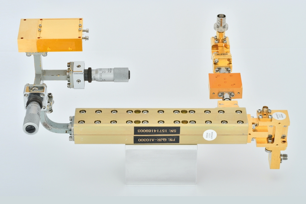
While we focused on additional optimisation of our packaging to improve the reliability of our IMPATT diodes, our collaborators from QuinStar Inc. engineered a microstrip cavity (see Figure 7(a)) that enabled us to measure IMPATTs more systematically without complex packaging requirements. This is a valuable adaptation, as short-loop feedback and device insight are very important when pursuing research and development.
We have mounted our 100 µm-thick GaN IMPATT diode in our microstrip cavity circuit and carried out tests under pulsed mode to reduce the thermal stress in the device. We started to capture oscillation with our spectrum analyser when we increased our bias current beyond 4.9 kA cm-2. By varying the biasing current density, we can tune the oscillation frequency from 28.8 GHz to 38.0 GHz. This tuning is a characteristic of IMPATT operation.
Benchmarking the power-frequency performance of our devices among experimentally reported GaN IMPATT oscillators produces encouraging results (see Figure 7(d)). We have recorded the highest oscillation at 38 GHz with an output power of 7 dBm. We attribute this success, involving entry to the Ka-band, to our thinning strategy that reduces series resistance and our tailored oscillation circuitry. It’s important to note that our microstrip cavity measurement provides a lower limit for device performance. That’s because compared with a waveguide resonate cavity, there is more parasitic loss in the circuit and reduced thermal dissipation in the diodes.

Figure 6. The waveguide resonate cavity and its simplified equivalent circuit under free-running oscillation.
Next steps
During our measurement process, we noticed that when continuously increasing the biasing current density, our devices suffered from overheating and an irreversible breakdown. This poses a challenge, as our theoretical and simulation analysis projects that we need to apply a biasing current density of more than 80 kA cm-2 to reach W-band oscillation. Based on these observations, it is clear that we must overcome thermal limitations, in order to realise higher-frequency oscillations with higher output powers.
To take on this task, we are now trying to resolve the reliability issues associated with our flip-chip-style packages. Previously, it has been shown that by flip-chip bonding silicon IMPATT diodes to a diamond heat sink, they can be prevented from burning out under input power densities up to a few MW cm-2. We expect that this state-of-the-art thermal solution can also aid GaN IMPATT diodes, once they have been optimised.
However, we should keep in mind that our GaN IMPATT diodes will operate under a much higher input power density than those made from silicon at a given frequency. Due to this, cooling demands are far tougher to meet. To do so, we will need to evaluate all the available techniques in our toolbox, to ensure that our GaN IMPATT technology will not be prohibited by self-heating of the device.

Figure 7. (a) A microstrip cavity circuit and an RF measurement setup. (b) Oscillation frequency versus biasing current density. (c) Peak output power versus oscillation frequency. (d) A benchmark plot of experimentally achieved GaN IMPATT oscillators.
It is possible that the development of diamond as a heat-spreading material, as well as the use of a thermally conductive substrate, could provide us with some inspiration. In addition to flip-chip packaging to a diamond heat sink, we will need to consider encapsulating the GaN IMPATT with a diamond heat spreader, and create diamond thermal vias to connect the hot spot to the heat sink. While there is still much work to do, we have already made much progress. Our key milestones include demonstrating the first Ka-band GaN-based IMPATT oscillator, a triumph that is supported by establishing a GaN substrate thinning process.
Our next steps, required to fully realise GaN’s promising potential for this technology, will centre on electro-thermal co-design. Success will unlock the door to GaN IMPATT diodes that combine higher frequencies with higher powers.