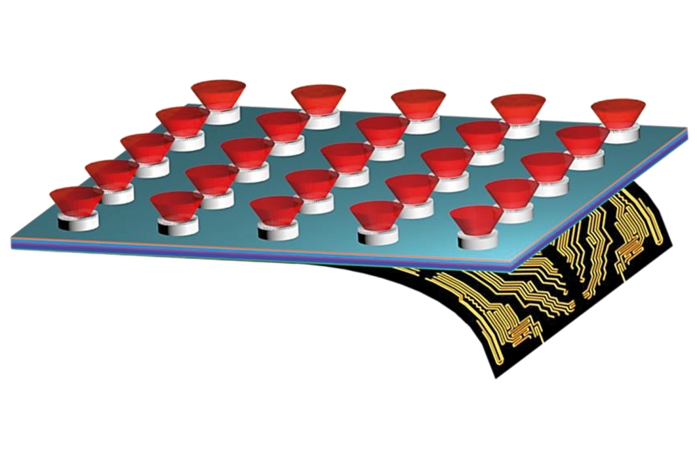
Monolithically integrated QCLs on silicon
Low-strain quantum cascade lasers with optimised metamorphic buffer
layers are closing the gap to realising reliable, high-power, infrared
sources on silicon
BY Enrique Sanchez Cristobal, Ahmad Azim and
Luke Millbocker from IRGlare, Matthew Fetters, Amy Liu and Joel Fastenau
from IQE, and Alejandro Villalobos meza and Arkadiy Lyakh from The
University of Central Florida
For designers of semiconductor lasers, quantum wells are a fundamental building block for these nanoscale devices, as well as an incredible asset. Not only do these devices serve as effective generators of laser light through radiative recombination processes, but the use of quantum well engineering also allows for control of emission wavelengths through changes in material composition.
Common semiconductor lasers, such as laser diode and the VCSEL, emit at wavelengths determined by the difference between the lowest energy levels of the electrons in the conduction band and the highest energy of the holes in the valence band of the quantum well material. This is a limitation that can be overcome by another unique semiconductor structure, the quantum cascade laser (QCL), which achieves lasing through inter-sub-band transitions associated with different excited states of the conduction bands of two materials. (see Figure 1).

Figure 1. Optical transitions in laser diodes (left) and QCLs (right).
While transitions in laser diodes are limited by the tuneability of the
material band gap, QCL optical transitions occur between excited
conduction band states of two materials which make up a periodic quantum
well structure. Engineering of these layers and their compositions
allow QCLs to emit light in the range of 3-14 µm.
At the heart of this semiconductor device is a superlattice composed of two alternating materials whose conduction bands work together to create a periodic quantum well structure, which emits infrared photons under an applied electrical bias. The material composition of the superlattice constituents can be varied to achieve emission in a broad infrared range, and the periodic nature of this structure enables a single electron to generate multiple photons as it cascades through the superlattice (see Figure 2).

Figure 2. Diagram of a stage, or period, of the periodic quantum well
structure that is generated from the conduction bands of the two
alternating superlattice constituents. Injected electrons experience
optical transitions before undergoing several non-radiative transitions
and reaching the end of the QCL stage. Electrons are then injected into
the next stage, where they repeat the process and continue to generate
infrared photons.
While QCLs are not as well-known as diode lasers and VCSELs, they are produced commercially, and are used in a range of critical sectors, including defence, spectroscopy, and free-space communication. In these applications they serve as compact, high-powered infrared sources that span the mid- to long-wave infrared range, thanks to a highly tuneable quantum well superlattice structure. More recent designs can deliver a continuous-wave output power of several watts at room temperature, enabling them to play pivotal roles in applications such as defence, where their low atmospheric losses at critical spectral windows allow them to be used in direct infrared countermeasure systems. Another important application is in the field of imaging, where QCL-based infrared microscopy has been successfully deployed for the rapid, precise classification of different cancer tissues.
Up until now, QCLs have usually been produced with lattice-matched material systems, such as InP. However, while this is conducive to maximising material quality and device performance, it also significantly limits the opportunities for this device, due to the high cost and low scale of native substrates.
The solution to overcoming this limitation is to modify the fabrication of QCLs to be able to account for the lattice mismatch between non-native substrates and the active layers. In this regard, our team at IRGlare, working in partnership with engineers at The University of Central Florida and IQE, has broken much new ground. Our triumphs include the first demonstration of monolithic integration of QCLs onto lattice mismatched substrates, and pioneering efforts related to the growth of these lasers on silicon. We are one of two groups to provide the first demonstration of integration of QCLs onto silicon – our team and another reported this success around the same time – and we trailblazed the integration of these lasers onto large-diameter silicon substrates. Another noteworthy claim of ours is that, until recently, our QCLs on silicon produced the highest performance on this foundation.

Figure 3. The metamorphic buffer design for a medium-wave infrared QCL
on silicon alleviates strain from lattice mismatch by gradually
transitioning the lattice constant between adjacent materials along the
growth direction.
Silicon integration
In the remainder of this article, we detail our efforts at producing high-performance QCLs on silicon. These lasers employ an InP cladding, surrounded by an active region that’s composed of alternating InGaAs and AlInAs layers that serve as quantum wells and barriers, respectively. By adjusting the composition of these materials, we either match the lattice-constant to the surrounding InP, or we target zero accumulated strain to maximise the quality of the epitaxial material – a crucial factor in ensuring laser performance.
One of the big attractions of growing QCLs on silicon is the opportunity to take advantage of the scalability and cost-efficiency of silicon technology. Thanks to the ubiquity of silicon in modern electronics, substrates made from this material are cheaper and far more accessible than the InP substrates that III-V-based QCLs traditionally rely on for good performance. Realising the direct epitaxial growth of QCLs on large-diameter silicon substrates offers the tantalising prospect of manufacturing compact infrared platforms that support both the electronic and photonic components on a single chip.
As well as the technical benefits of integrating complex components on a single compact chip, silicon substrates offer the benefit of massively upscaling the production and yield of standard QCLs, as silicon wafers with diameters that are larger than 200 mm are readily available. These large-diameter wafers, coupled with the exceptionally compact nature of standard QCLs, promise to enable the processing of significantly more QCLs on a single wafer, all while reducing the cost of production.

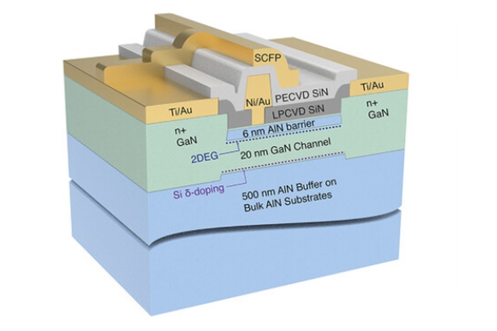
Figure 4. Waveguide design of a third generation long-wave infrared QCL
structure, produced on a silicon substrate, employs an improved
metamorphic buffer and a lower-strain active region.
While success on this front would be a wonderful evolution for QCL technology, standing in the way is a significant hurdle. If this technology is to be viable, it is vital to reconcile the substantial lattice constant mismatch between InP and silicon. A threat that’s faced when undertaking the epitaxial growth of InP QCLs on lattice-mismatched substrates is the creation of defects in the material that propagate through the epitaxial layers to reach the laser core, where they degrade device performance and reliability. However, despite this complication, researchers have produced QCLs on non-native substrates, with efforts currently focused on bridging the gap and delivering the performance that QCLs provide on native substrates.
One way to partially address the issue of lattice mismatch is to introduce metamorphic buffer layers, which gradually transition the lattice constants between adjacent layers of different materials during epitaxial growth. By slowly adjusting the lattice constant, it is possible to trim the density of defects that can hinder laser performance and reliability (see Figure 3).
Our initial efforts to integrate QCLs on lattice-mismatched substrates began with GaAs substrates, which have a lattice mismatch of 4 percent with InP – half that of silicon. We produced a mid-wave infrared QCL with a highly strained laser core, incorporating a metamorphic buffer to drive down the defect density in the active region. These ridge-waveguide lasers operate at room temperature. Despite the lattice-mismatch, initial processing runs provided a good yield.
Building on this work, we monolithically integrated this design on a 150 mm germanium-coated silicon substrate template, utilising a graded InAlAs metamorphic buffer. These QCLs lase up to 170 K, but yield is low, and these devices consistently experience degradation after only 30 minutes. According to material characterisation of these preliminary designs, to ensure a good performance on silicon, strain in the material must be reduced. Options to realise this include introducing a low-strain laser core design and improving the metamorphic buffer designs.

Figure 5. (a) Pulsed light-current-voltage (L-I-V) plots for a
third-generation QCL. This device reached a maximum power of around 3 W.
(b) M2 measurements determine the deviation from a perfect gaussian
beam, with M2 =1 denoting a perfect gaussian beam. A high quality
single-lobed beam was measured. (c) Pulsed light-current-voltage for
multiple third-generation devices shows excellent short-term
reliability.
Drawing on these initial attempts, more recently we produced a third-generation laser, this time emitting in the long-wave infrared range. This ridge-waveguide QCL design combines reduced strain in the laser core with an improved germanium-coated silicon substrate featuring a reduced defect density. Our design employs a modified metamorphic buffer, formed from interleaving GaAs and AlInAs layers, and an additional InGaAs layer beneath the InP cladding (see Figure 4). For this QCL, we use a 200 mm wafer, the largest in this analysis.
Our third-generation design delivers a dramatic improvement over the second-generation variant. Our successor boasts a good performance, delivering 3 W of pulsed power at room temperature, and according to M2 parameter tests, provides a good gaussian beam quality (see Figure 5). In addition, our third-generation QCL provides excellent reliability, with no signs of degradation after 10 hours of operation at maximum power. Another encouraging observation is a good yield of functional devices. What’s more, we can make many more laser chips from a single substrate, compared with what may be typically harvested from smaller InP substrates.
Based on all these merits, our QCL shows great promise for the future of this class of laser on silicon. Our findings illustrate the impact of improving material quality through low-strain laser core designs and improved metamorphic buffers.

Figure 6. (004) Reflection high-resolution X-ray diffraction spectra for the four samples discussed in this work.
Characterising material quality
The strengths of our third-generation design are evident in the materials characterisation of a range of structures. We have compared this third-generation silicon-QCL heterostructure to older generation mid-wave designs grown on InP, GaAs and silicon – the latter substrates have lattice-mismatches with InP of 4 percent and 8 percent, respectively.
As expected, X-ray diffraction reflection spectra of the lattice-matched sample show sharp superlattice satellite peaks, indicative of high crystal quality (see Figure 6). The positions of these peaks confirm that the superlattice period is within 1 percent of the expected value. For all the structures with lattice mismatch, there is a broadening of the diffraction peaks, preventing the gauging of the superlattice period. Despite this, the diffraction peaks of the lattice-mismatched samples reflect a successful transition of lattice constants from silicon to InP, as indicated by the distinct peaks of each alloy present in the spectra.

Figure 7. Atomic force microscopy surface roughness images for a 20 µm
by 20 µm area of (a) first-generation, (b) second-generation and (c)
third-generation structures. Note that the first-generation structure is
grown on a GaAs substrate, while second and third-generation structures
are grown on silicon substrates.
A major challenge facing every grower of QCL structures on mismatched substrates is maintaining a smooth surface required for device processing and operation. We have investigated surface morphology with atomic force microscopy, considering values of root-mean-square surface roughness for scans over a 20 µm by 20 µm area. We find our QCLs lattice-matched to InP have the smallest surface roughness, never exceeding the thickness of a single monolayer (0.1-0.2 nm). Lattice-mismatching increases surface roughness, with values of 3.2 nm and 22.3 nm, respectively, for mid-wave emitting active regions grown on GaAs and silicon. However, refining the growth of the metamorphic buffer and the bottom cladding layers – these are the improvements introduced in our third-generation QCL – delivers a reduction in surface roughness to 4.9 nm (see Figure 7). This observation provides further evidence of the benefits of our latest design.
To understand the impact of the metamorphic buffer on defect suppression, we have scrutinised our samples with transmission electron microscopy, a technique that enables high-resolution imaging of defects in crystalline structures. This form of microscopy shows that the metamorphic buffer helps to reduce the defect density in the active region around structures grown on silicon. However, in the structure associated with our second-generation QCLs, large defects are present within the active region, as well as in the surrounding cladding material. In stark contrast, no defects are spotted in or around the active region of the QCL on native InP (see Figure 8). Such findings are consistent with the poor reliability of our second-generation QCLs.

Figure 8. Transmission electron microscopy images of an active region of
a QCL grown on a native substrate (left) and the second-generation QCL,
grown on silicon (right). The active region of the QCL grown on a
native substrate (InP) appears entirely devoid of any defects, while the
active region of the second-generation QCL has large linear defects,
evident on the cladding and within the laser core (encircled).
Another insight provided by transmission electron microscopy is the level of effectiveness of the modified metamorphic buffer in reducing defect density. In our third-generation QCL, defects originating at the Si-Ge/GaAs interface are reflected back into the substrate. It is also worth noting that while defects persist in the cladding layers, the active region is devoid of large-scale defects that plague our second-generation QCLs (see Figure 9).
Quantifying defect density is ineffective when inspecting samples ‘head-on’ with transmission electron microscopy, because this leads to a limited view of the surrounding cladding. It is more informative to turn to plane-view imaging to determine defect density in specific regions. By taking this approach (see Table 1 for the results of our analysis), we have found that the defect density in our third-generation QCLs exceeds both the first- and second-generation variants, and is beaten in this regard only by QCLs on native InP substrates. We view this result as incredibly promising, demonstrating a substantial improvement in the realm of lattice-mismatched substrates that will inform future QCL designs.
Through our efforts we have solidified the connection between higher-quality material and more-reliable, high-performance QCLs on non-native substrates. The performance of our third-generation QCLs, produced on 200 mm wafers, provides proof of the innate scalability and cost-efficiency when transitioning to this foundation. By switching to a silicon substrate, we create high-quality devices on a wafer that is more cost-effective and has the potential to yield four times the number of functional devices that can be realised on 50 mm InP wafers.

Figure 9. (Left) Transmission electron microscopy image of epitaxial
layers of the third generation of QCL, grown on silicon. Inspecting the
metamorphic buffer, circled in red, reveals that very few defects
propagate past this buffer and into the mostly intact InGaAs layer.
(Right) Transmission electron microscopy image of the active region and
surrounding InP cladding of the third-generation QCL shows that it is
devoid of the large-scale defects previously seen in the
second-generation QCL, also grown on silicon.
While much progress has been made, we are not resting on our laurels. Instead, we are striving to improve the design and optimisation of metamorphic buffers, as well as the overall quality of silicon substrates. However, our results represent a clear step towards marrying the high performance and versatile spectral range of QCLs with the accessibility of silicon-based platforms.

Table 1. The defect density found in QCL structures produced on a range of substrates.
Our ultimate goal is to integrate QCLs on silicon without compromising their performance, so they are as good as they are on a native foundation. Another aim, building on our success with QCLs-on-silicon in the long-wave infrared, is to replicate these results in the mid-wave infrared. To excel in this regard, we will have to employ design techniques such as lower-strain superlattices and reduced stage numbers, as well as placing greater emphasis on ensuring sufficient strain-reduction through strain-balancing the quantum wells and barriers. If we succeed, we will pave the way for game-changing infrared platforms, while further cementing QCLs as indispensable infrared solutions for myriad applications.
• Conflict of Interest Statement: Arkadiy Lyakh owns stock in IRGLARE, LLC and as such may benefit financially as a result of outcomes of the research or work reported in this publication.
• Acknowledgement: This work was supported by the Naval Air Warfare Center Weapons Division, China Lake, CA, under Grant N6893622C021. (Corresponding author: Arkadiy Lyakh.)