GaN nanowires on a silicon platform eye novel optoelectronics
Nitride nanowires with a large surface-to-volume-ratio offer intriguing
optoelectronic properties that could advance integrated photonics.
BY HUABIN YU, YUANMIN LUO, WEI CHEN AND HAIDING SUN FROM THE UNIVERSITY OF SCIENCE AND TECHNOLOGY OF CHINA
One-dimensional semiconductor nanostructures, such as single-crystalline nanowires, are the key ingredient in emerging nanoscale optoelectronic devices. These miniature marvels promise to play a variety of roles, including serving in the ultimate form of integrated photonics.
It is possible to produce nanowires with a range of materials. They include the group III-nitrides, which offer direct and tuneable bandgaps. Nanowires made from this material system offer single-crystalline quality, realised through MBE growth that allows for full strain relief during the epitaxial process. Additional merits of nanowires, when produced by MBE, are precise morphology and size control - and thanks to a large surface area, an exceptional light absorption efficiency and light extraction efficiency.

Figure 1. The Photoluminescence spectra of (a) the pristine nanowires
and (b) nanowires coated with quantum dots. The scanning electron
microscopy image of GaN/AlGaN nanowires on a silicon substrate (c)
without a coating of quantum dots and (d) with a coating of quantum
dots. The scale bar is 1 µm. The electroluminescence spectra of the
nanowire device (e) without quantum dots, (f) and with quantum dots
under injection currents of 20 mA to 100 mA. Insets of (e) and (f) show
optical images when the devices are emitting light.
This wonderful set of attributes makes III-nitride nanowires a compelling candidate for a number of optoelectronic devices. These nanoscale structures could play a crucial role in LEDs, photodetectors, laser diodes, and even photoelectrochemical devices for chemical/biological photoelectronic sensors. Exploring all of these possibilities and more is our team from the iGaN Laboratory at the University of Science and Technology of China.

Figure 2. (a) The current-voltage (I-V) characteristics, (b) the
responsivity as a function of wavelength, and (c) the colour contour
plot of the spectral response matrix of broadband photodiodes. Incident
light intensities of the deep-UV and near-IR light are 100 µW.
Photocurrent responses of the photodiodes operating at (d) under 254 nm
light, and (g) under 800 nm light. Representation of response time and
decay time interval of the broadband photodiodes under (e) 254 nm and
(h) 800 nm light. The incident light intensity is 100 µW. Photocurrent
of the devices under (f) 254 nm light and (i) 800 nm light with various
light intensities from 10 µW to 100 µW.
GaN nanowires for LEDs ….
GaN nanowires hold much promise for increasing the efficiency of the LED, thanks to properties that are superior to those of planar structures. One key merit of the GaN nanowire is that it can be grown directly on silicon or another foreign substrate, while offering an internal quantum efficiency that’s enhanced through effective lateral stress relaxation during the epitaxial growth process. What’s more, this class of nanowire increases p-type doping efficiency, due to a reduced activation energy of the magnesium dopant in nanowire structures. There are also the benefits of a large surface-to-volume ratio and multiple scattering effects, assets that facilitate a high light-extraction efficiency. And on top of all of this, the large surface area of III-V nanowires opens the door to integration with various low-dimensional functional materials, including colloidal quantum dots. This leads to many tantalising prospects surrounding the future of multifunctional integrated photonic chips and optoelectronic systems.
In our iGaN Lab at the University of Science and Technology of China we have developed a broadband nanowire LED that produces emission that spans the UV to the red, via the integration of colloidal quantum dots (see Figure 1 (a) for the photoluminescence spectra of bare nanowires, and Figure 1 (b) for those coated with quantum dots).

Figure 3. An illustration of the photoelectrochemical device based on GaN nanowires.
We have investigated the morphology of our bare and coated nanowire arrays with scanning electron microscopy (see Figure 1 (c) and (d)). Images indicate that the colloidal quantum dots uniformly reside towards the top of the nanowire array.
Our work has extended to evaluating our nanowire LEDs under electrical bias. These devices exhibit rectification behaviour and a sharp electroluminescence peak around 325 nm (see Figure 1 (e)). The addition of colloidal quantum dots pushes the electroluminescence peak to 600 nm (see Figure 1 (f)).
…photodetectors…
As stated already, GaN nanowires can be grown on various substrates with a near defect-free material quality, thanks to efficient strain relaxation that’s associated with the one-dimensional geometry. It’s an asset that enables our nanowires to be directly grown on a silicon substrate without a buffer layer, and ensures direct carrier transport between the GaN nanowires and silicon. Due to this, GaN nanowires on silicon sidestep the challenges faced when trying to realise the monolithic integration of III-V semiconductors with silicon photonic systems.
Drawing on this favourable situation, we have developed an integrated tuneable broadband light-detecting device that employs III-V nanowire/silicon heterostructures. Our design demonstrates a bias-controlled switchable operation mode, and enables extreme broadband photodetection as well as self-powered narrowband photodetection.

Figure 4. (a) A diagram of the photoelectrochemical photodetector
optical communication system. (b) Demonstration of reprogrammable binary
and ternary optoelectronic logic gates based on a photoelectrochemical
photodetector. (c) Demonstration of an encrypted optical communication
system. (d) The mechanism for a photoelectrochemical glucose sensor.
When we operate our device under zero or negative bias, our photodetector can realise a built-in electric field from the n-region to the p-region, or utilise an external electrical field from the bias. Photocarriers that are generated under optical excitation are driven by these electrical fields, causing electrons and holes to move in opposing directions. It is this mechanism that enables the device to function in photo-detection mode (see Figure 2 (a)).
Note that our device demonstrates a broad response under reverse bias, transitioning to narrowband photodetection in the deep-UV under zero bias, where the off-rejection ratio (R254 nm/R800 nm) is very high, exceeding 106. We have also recorded bias-dependent spectral response curves (see Figure 2 (b)) and the matrix (Figure 2 (c)), results that further validate the ability of our photodetector to switch between broadband and narrowband operation.
We are encouraged by the competitive responsivity of our devices. This is evident in the UV region, where they are comparable to commercial broadband silicon photodiodes, such as the Thorlabs PDA10A2. According to square-wave photo-responses, our device demonstrates a rapid response under deep-UV/near-IR illumination (see Figures 2 (d) and 2 (g)). The response speed, evaluated in terms of the rise time, is 45.5 ms and 29.4 ms for illumination under deep-UV and near-IR light, respectively. The primary reason for the more rapid response at a longer wavelength is the narrower active region (intrinsic layer) between AlGaN and silicon, in comparison with the AlGaN multi-quantum-well region. However, there is a price to pay for this advantage, with the relatively thin active region of AlGaN/silicon leading to lower responsivity, and resulting in a saturated photocurrent under a high near-IR light intensity (see Figures 3 (f) and 3 (i)). Care is needed when considering this trade-off between the responsivity and the response speed, with the decision needing to take into account the total area for light absorption and response characteristics.

Figure 5. (a) The imaging system setup. (b) A filterless colour discrimination system. (c) Broadband multi-colour system.
…and photoelectrochemical devices
As well as traditional optoelectronic devices, already described, we are able to produce novel, high-efficiency, photoelectrochemical devices (see Figure 3). One of the reasons that this opportunity arises is because we can tune the optical and electrical properties of our GaN nanowires, due to their physically confined structures and large exposed surfaces. What’s also crucial is that these nanowires exhibit environmentally sensitive surface properties, enabling the operation of photoelectrodes in specific aqueous environments.
Our photoelectrochemical devices employ a GaN nanowire array as the working electrode, and a platinum mesh as the counter electrode. When operated in electrolytes and illuminated by deep-UV photons, electrons and holes are excited in the working electrode, the GaN nanowires. Driven by the downward band-bending at the interface between the GaN nanowires and the electrolyte, the photo-generated electrons drift to this interface, to undergo the following redox reactions in the electrolyte: 4H+ + 4e- = 2H2. Another consequence of the band bending is that it induces the directional transfer of holes in the opposite direction, towards the platinum counter electrode, through the external circuit. In this case, the reaction is 2H2O + 4h+ = O2 + 4H+. The H+ ions that are created diffuse through the electrolyte to reach the counter electrode and form the whole circuit. During operation, the device’s photocurrent is read out by the electrochemical workstation.
The success that we have had is noteworthy, given that photoelectrochemical devices, which have unique working principles that combine semiconductor physics with a chemical reaction process, are attracting extensive interest by combining simple fabrication with low cost, self-powering and appealing electrolyte-assisted device properties. Thanks to their electrolyte-assisted operating characteristics, as well as following the conventional carrier-generation, separation, and migration processes in semiconductors, these photoelectrochemical devices have a procedure that involves a redox reaction at the semiconductor/electrolyte interface – this equips us with more freedom to regulate the photo-response behaviour.
Due to this promise, our iGaN Lab has unleashed the potential of GaN nanowire-based photoelectrochemical devices in a number of fields, including underwater optical communication, optoelectronic logic, artificial vision, automatic imaging, energy-conversion catalysis, and biosensors (this is illustrated in Figures 4 (a-d)).

Figure 6. (a) 3D schematic, (b) circuit diagrams, and (c) photograph of
the setup for the on-chip deep-UV/near-IR visualisation systems. The
photocurrent of the broadband photodetector (PD) is converted to voltage
with a trans-impedance amplifier (TIA). (d) Demonstration of the
deep-UV/near-IR visualisation systems for early warning systems. (e) The
information of the encoded visible light signals when the system is
operating to detect deep-UV signals.
Investigating opportunities
To explore the potential applications of our newly developed devices, we have integrated them in a diverse range of optoelectronic systems. We began by building an imaging system for broadband image recognition and classification (see Figure 5 (a)). This features a range of LEDs emitting at different wavelengths as the light source, and a mask displaying the seal character ‘USTC’ positioned between the light source and the broadband nanowire photodetector. In this system, the bottom broadband nanowire photodetector records light signals as the mask undergoes scanning in both horizontal directions.
By recording photocurrent data at different biases at each mapping position, we have generated a spatial response data cube for image recognition and classification. When we operate the device in a narrowband mode by applying a 0 V bias, we obtain a blurred pattern with 800 nm light. However, when we turn to 254 nm light, this ensures a distinguishable illuminated pattern (see Figure 5 (b)).
Switching to a broadband mode, realised by applying a negative bias, enables our system to deliver multi-colour imaging. Under this condition, there are discernible patterns of the ‘USTC’ seal character with deep-UV (254 nm) and near-IR (800 nm) light sources (see Figure 5 (c)), showcasing our device’s capability for image recognition and classification across both the deep-UV and near-IR spectral domains.
Following on from the successful merger of two nanowire devices on a single silicon platform, we created a versatile deep-UV/near-IR visualisation system. Here one device acts as a broadband photodetector and the other as a visible emitter (see Figure 6 (a-c) for the system’s schematics, circuit diagrams, and photographs, respectively).
To demonstrate the functionality of this system, we employ a visible-blind signal source by pairing a commercial LED with a UV lens. In this configuration, the light intensity of the LED serves as an analogue input signal. When the broadband nanowire device detects UV or near-IR light a corresponding photocurrent results. These signals are simultaneously converted and amplified with a trans-impedance amplifier, with the amplified voltage signals modulating a visible emitter with a consistent bias. The emitted visible light is collected and recorded by a spectrometer system, using a fibre.
The output that results from using UV light as the input signal (see Figure 6 (e)) demonstrates that this integrated system can function as an early warning system. For example, a red alarm light signal can highlight that someone has entered a dangerous area, while using an invisible light signal to prevent potential injury (see Figure 6 (d)). By successfully integrating nanowire devices in a UV/near-IR visualisation system, we are showcasing its potential for multifunctional applications in smart optoelectronic systems.
Our vertically integrated III-V nanowire architectures on the silicon platform holds great promise for future monolithic integrated multi-component photonic systems with simpler, cheaper hardware. So far, we have demonstrated a bias-controlled, multifunctional broadband emitting-detecting device that seamlessly integrates III-V p-n nanowires onto a silicon platform. This novel device offers remarkable functionalities, including tuneable detection and emission across a wide spectral range, spanning the deep-UV to the near-IR. This progress creates monolithically integrated multi-component photonic systems that feature reduced hardware complexity and cost.
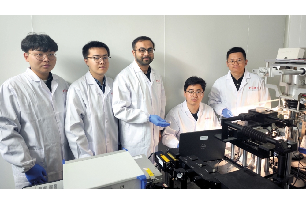
Main image: The iGaN Lab team from the University of Science and Technology of China, led by Haiding Sun and including his PhD student Huabin Yu and members who contributed to this work.