DUV micro-LED array advances maskless photolithography
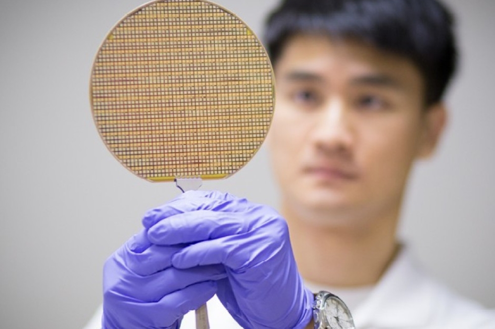
A team led by Sun Haiding from the University of Science and Technology of China (USTC) has developed a vertically integrated micro-LED array which was then applied in deep ultraviolet (DUV) maskless photolithography system for the first time. Their study was published in Laser & Photonics Reviews.
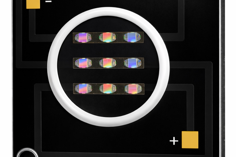
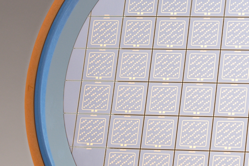
Sun’s iGaN team designed and optimised the epitaxial structure, size, sidewall profile, and shape of the DUV micro-LED, to improve power efficiency, modulation bandwidth, and functionality in UV light detection, imaging and sensing. Building upon this, the team then developed an array system based on the micro-LEDs.
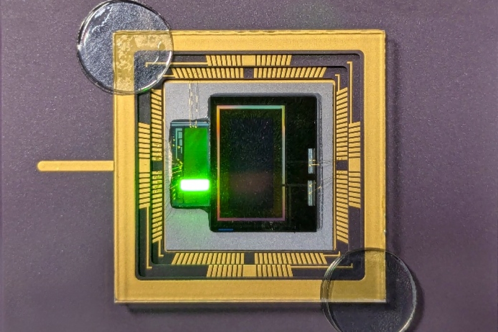
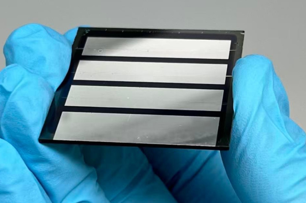
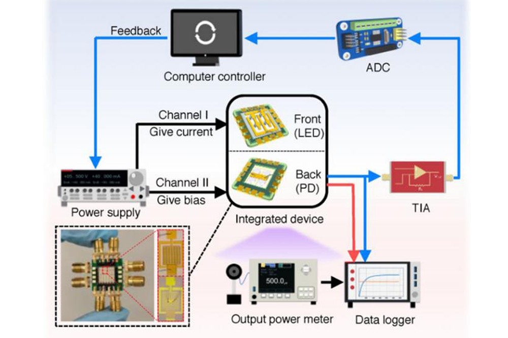
The team then developed a DUV display integrated chip, building on the advantages of DUV micro-LED’s ultra-small size and ultra-high brightness. They proposed a 3D vertically integrated device architecture with a AlGaN-based DUV micro-LED array and zinc oxide (ZnO)-based photodetector (PD) side-by-side via a transparent sapphire substrate.
With this architecture, the UV photons emitted from the DUV micro-LED array can penetrate the transparent sapphire substrate and be captured by the PD on the backside of the substrate, enabling efficient optical signal transmission.
Furthermore, the team developed a self-stabilising luminescence system with a closed-loop feedback control based on the vertically integrated device. This system can not only monitor fluctuations of the output light intensity of the micro-LED array, but also provide continuous feedback to ensure stable output power.
Test esults showed that the device with self-stabilising system maintains high light intensity and long-term stability while the light intensity of the device without feedback gradually decreased over time.
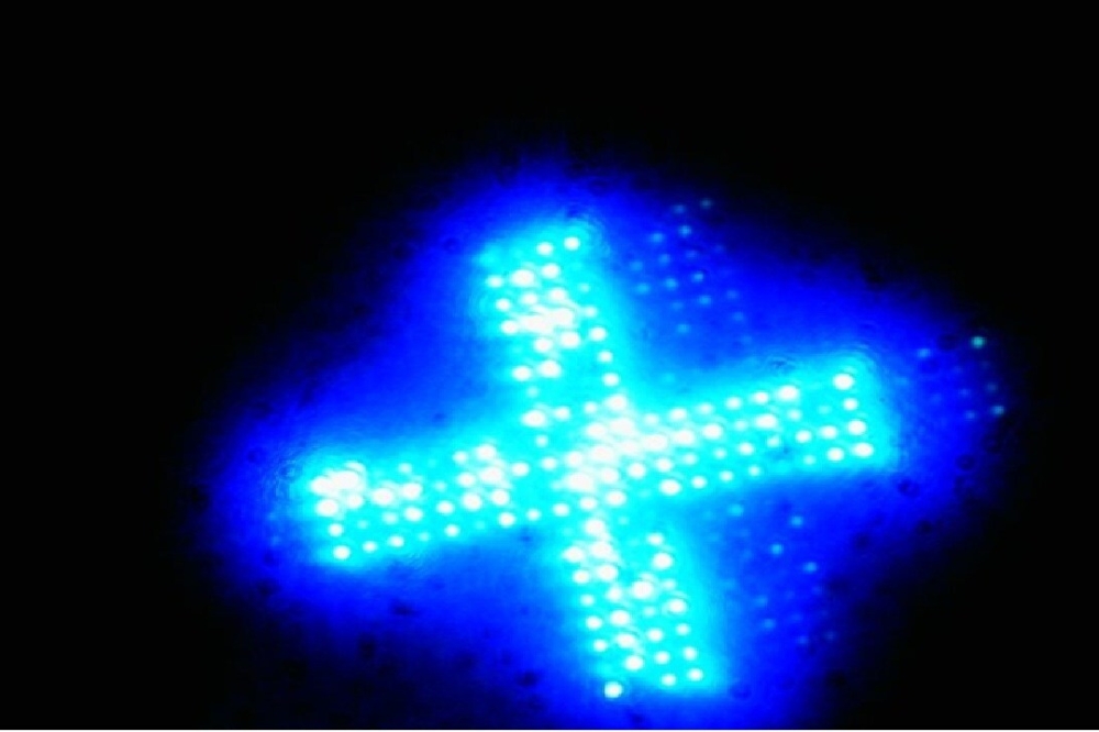
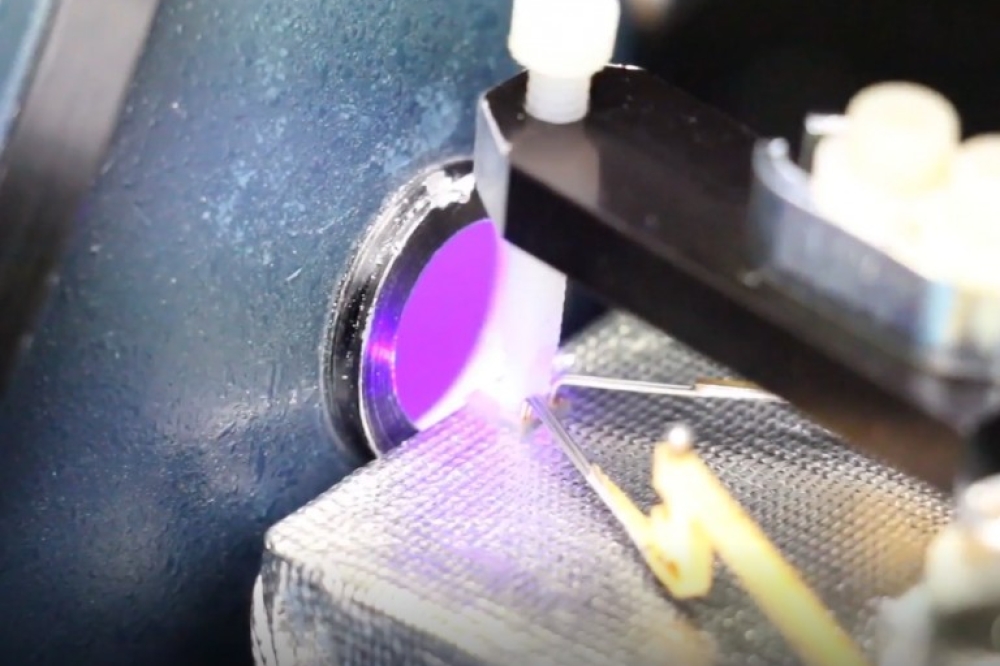
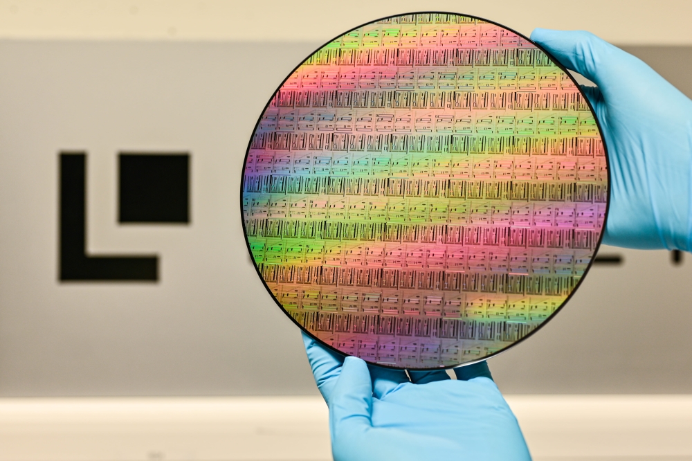
Using the feedback system, the team demonstrated a DUV micro-LED array with a pixel density of 564 pixels-per-inch (PPI) and successfully displayed a clear pattern on a silicon wafer after the maskless DUV photolithography, indicating potential in high-resolution photolithography technology. This is the first demonstration of DUV maskless photolithography based on a DUV micro-LED active matrix.
The team believes this novel device has significant application prospects for future maskless photolithography system. It also lays the foundation for the future development of highly integrated and multifunctional 3D optoelectronic integration systems.
In the next phase, the team will focus on further reducing the size of individual micro-LED and PD, to increase the density and integration of arrays per unit area. They will also optimise the performance of individual devices and the uniformity across large wafers, paving the way for higher precision in maskless photolithography technology.

