A red revolution with quantum machine learning
Quantum-mechanical modelling and machine learning can accelerate the
design of semiconductor devices, such as polychromatic LEDs based on
InGaN
BY NICK PANT FROM THE UNIVERSITY OF TEXAS AT AUSTIN
At the heart of humanity’s digital revolution is device miniaturisation. Efforts began with the scaling of the transistor, shrinking at a rate described by Moore’s law. Now the LED is following suit, with these miniature marvels promising to unleash a new generation of display technologies that seamlessly blur the lines between reality and virtual reality. Due to this, there are tremendous opportunities for microLEDs in mini projectors in mobile phones, as well as in 3D near-eye glasses and other applications, where they will deliver a tremendous improvement to wearable displays. Such advancements will reshape our interactions with the digital world by influencing how we consume media, access education, and connect with our colleagues.
However, we should not get ahead of ourselves. While miniaturisation of the LED holds much promise, its execution poses significant engineering challenges.
One of the greatest obstacles to success is related to the materials that are used to produce these emitters. Blue and green LEDs are made with InGaN quantum wells (see Figure 1 (a)), while those that emit in the red feature quantum wells made from InGaP. These two classes of semiconductors have entirely different crystal structures, with lattice constants that differ by 30 percent – for epitaxial growth, that’s an enormous disparity. Due to this, it is exceedingly difficult and expensive to create monolithic micron-scale pixels by integrating red InGaP LEDs with their green and blue InGaN cousins.
Figure 1. (a) At the heart of an InGaN LED are InGaN quantum wells,
buried within a GaN p-n junction. These devices often feature an AlGaN
barrier, used to prevent the overflow of electrons from the quantum
well. (b) Calculated luminescence spectra of InGaN quantum wells as a
function of the indium concentration, denoted above each curve, showing
that the wavelength can be tuned across the visible spectrum.
An alternative way forward is to produce red, green and blue LEDs with one material system. Take this route and there’s only one choice, InGaN – it is the only commercially proven semiconductor with a bandgap that can be compositionally tuned across the entire visible spectrum. To propel its emission to longer wavelengths, engineers have to increase the indium content in the well, as this narrows the bandgap (see Figure 1 (b)). Producing an all-InGaN polychromatic pixel is viewed as the holy grail of microLED research, because it circumvents all the difficulties associated with integrating InGaP with InGaN.
Unfortunately, the light-emission efficiency of InGaN plummets with increasing wavelength. For even the best red LEDs, more than 80 percent of the current is dissipated as heat. Consequently, it is essential to uncover the mechanistic origins of InGaN’s performance, as this promises to unlock the door to realising efficient polychromatic microLEDs.
As mechanistic insights into fundamental material bottlenecks are difficult to access experimentally, quantum mechanical calculations prove invaluable. This is the approach that I adopted as a doctoral candidate at the University of Michigan, developing quantum-mechanical methods to computationally model the performance bottlenecks of InGaN LEDs. These efforts, involving solving Schrödinger’s and Poisson’s equations for electrons and holes, have provided predictions based on first principles on how these carriers recombine to produce light in realistic LED structures.
Funding for this work came from the Department of Energy (DoE) Solid-State Lighting Program, a major catalyst for LED development in the US. This support allowed our research group, led by Emmanouil Kioupakis, to collaborate with one of industry’s most significant and pioneering LED manufacturers, Lumileds, as well as experimental researchers from the University of New Mexico, Ohio State University, and Sandia National Laboratories. This unique opportunity, in place for over five years, allowed our team to closely benchmark our calculations against experiments. Providing the critical foundation for this success, outlined in the remainder of this article, is decades of previous work by many scientists from around the world.
Figure 2. (a) InGaN crystallises in the wurtzite structure. With this
geometry, the dipole of the cation-nitrogen bonds do not cancel out
along certain directions. The arrow indicates the direction of the
dominant spontaneous polarisation, which is parallel to the c-axis used
for growth. (b) Band diagram of an InGaN/GaN quantum well, showing how
the internal polarisation field separates electron and hole wave
functions.
InGaN’s challenges
Broadly, InGaN’s challenges can be divided into two categories: extrinsic and intrinsic. The extrinsic bottlenecks stem from material imperfections, such as point defects and dislocations, that cause electrical energy to be lost to heat. It is difficult to grow high-quality InGaN with indium compositions exceeding 30 percent, the ballpark for realising red emission. However, thanks to innovations in growth and fabrication that will inevitably take place over the coming years, we can expect continuous improvement in the quality of InGaN.
Unfortunately, intrinsic bottlenecks are more difficult to control, because they are related to fundamental material properties. Intrinsic challenges like efficiency droop, which is the fall in light-emission efficiency with increasing current, plague the performance of InGaN emitters in the red and even the green. Another persistent challenge is a blueshift that occurs with increasing current density – it is not uncommon for red LEDs to turn yellow or even green when the current is cranked up through these devices.
Peculiar polarisation
Unlike the more conventional III-V systems, those incorporating InGaN quantum wells exhibit built-in polarisation fields that exceed 1 MV cm1. These fields originate from InGaN’s wurtzite crystal structure, where dipoles of the (In,Ga)-N bonds do not cancel out along certain directions (see Figure 2 (a)). When the indium composition of the quantum well increases, this strengthens the polarisation fields across the quantum wells. Consequently, red emitters, which are richer in indium, suffer from stronger fields than their blue-emitting siblings.
For many years, polarisation fields have been blamed for the decline in InGaN efficiency as emission is extended from the blue to the red. It’s been argued time and time again that by pulling apart electrons and holes, electric fields slow recombination (see Figure 2 (b)). But that’s only part of the story. The reality is that polarisation fields impede both radiative and non-radiative recombination. As the radiative efficiency depends on the ratio of the radiative to the non-radiative recombination rate, it is not possible for polarisation fields per se to explain the plummeting efficiency.
Shedding new light on this matter is the realisation that polarisation fields influence the operating carrier density of LEDs. When quantum wells are subjected to stronger polarisation fields, this slows recombination dynamics and results in the need for more carriers to realise a similar brightness, compared with quantum wells with weaker fields. Our modelling of blue, cyan, and green LEDs grown at Lumileds indicates that increasing the strength of polarisation fields produces a significant decline in the recombination rate and an increase in carrier density with increasing wavelength.
Figure 3. Radiative recombination involves the recombination of an
electron and a hole, leading to the spontaneous production of light.
Auger-Meitner recombination is a competing loss mechanism involving
non-radiative recombination of an electron and hole, with excess energy
exciting either a nearby electron (shown) or a nearby hole (not shown).
The increase in carrier density is detrimental to device performance. When too many carriers crowd the active region, they scatter off of one other, leading to a process called Auger-Meitner recombination. In this non-radiative process, the excess energy from an electron-hole recombination event leads to excitation of a nearby electron or hole, rather than radiative recombination. Since Auger-Meitner recombination involves three carriers, it scales cubically with carrier density. That’s more dramatic than radiative recombination, which scales quadratically, as it involves only two carriers (see Figure 3).
Due to this variation in scaling behaviours with carrier density, the non-radiative Auger-Meitner process overtakes radiative recombination to become the dominant process when the current is cranked up. Confirming this conjecture are the experimental measurements of carrier lifetime by our collaborators at the University of New Mexico, who concluded that this effect is the primary cause of efficiency decline from blue to green in state-of-the-art quantum wells.
According to our calculations, this issue is even more prevalent in red LEDs. In these nitride-based devices, the carrier density is orders of magnitude higher than it is in blue emitters. Due to this, it is crucial to cut the carrier density in long-wavelength InGaN LEDs, if they are to be efficient.
Refocusing on carrier density
Another significant challenge associated with longer-wavelength nitride-based LEDs is a blueshift with increasing current. To fathom the origins of this issue, one must understand that polarisation fields decrease the bandgap of quantum wells by causing a finite voltage to drop across its width.
The introduction of free carriers into the quantum wells decreases the voltage drop through the electrostatic screening of the fields. This has conventionally been the explanation for InGaN’s blueshift problem.
While intuitive, the established explanation is not complete. At high carrier densities, there’s a need to also account for band filling, which reflects the recombination of higher-energy electrons and holes deep within the conduction and valence bands. In addition, it’s important to include the spatial reorganisation of free carriers due to many-electron correlations – this leads to a compensating redshift in the emission energy, known as plasma renormalisation. By integrating all these effects, our quantum-mechanical calculations accurately predict the wavelength shift of green LEDs grown at Lumileds (see Figure 4 (a) and (b)).
What may come as a surprise is that the main contribution to the hue-shift problem is not a shift in peak wavelength but a broadening of the spectral linewidth. This broadening leads to the Abney effect, which occurs when two light sources with the same peak wavelength but different linewidths are perceived as different hues by the human eye.
Our calculations indicate that the broadening of the spectra at higher currents is a signature of an increasingly degenerate carrier density (Figure 4 (c)). Energy broadening comes from light emission from high-energy electron and hole states that are deep inside the conduction and valence bands, which would not be occupied at lower carrier densities.
Based on our observations, we advocate a reframing of the hue-shift problem. Rather than attributing the problem to individual effects, such as polarisation-field screening or band filling, we argue that the real culprit is the high carrier densities required for the operation of long-wavelength nitride LEDs. By reducing the carrier density, it’s possible to eliminate polarisation-field screening, band filling, and plasma renormalization.
To put it succinctly, we see efficiency droop and hue shift as two sides of the same coin, both resulting from excessively high carrier densities. By reducing the operating carrier density, it should be possible to significantly alleviate the intrinsic challenges faced by long-wavelength nitride LEDs.
Figure 4. (a) Electroluminescence spectra from a single quantum well of a
green LED grown at Lumileds, specially designed to allow for accurate
recombination lifetime measurements. As the current density increases,
the peak wavelength blueshifts and the spectral linewidth broadens,
leading to a net blueshift of the perceived hue. Calculations
quantitatively predict the peak-wavelength shift and the linewidth
broadening, quantified by the full-width at half maximum (FWHM). Figures
reproduced from AIP Advances 12 125020 (2022).
The combinatorial challenge
Identifying a high carrier density as the main issue in long-wavelength nitride LEDs has allowed us to explore suitable solutions. Our success has hinged on uncovering quantum-well designs that enable a reduction in the carrier density. To find device architectures that excels in this regard, we have been mapping out the space of possible quantum-well designs.
Despite the immense importance of III-nitride quantum wells – that’s those containing aluminium, indium and gallium – we have found that their design space remains largely uncharted. It’s a state of affairs that stems from the underlying combinatorial challenge. For instance, if we were to discretize compositions in units of 0.01, there would be more than 2.6 million combinations of AlxIn1-x-yGayN wells and barriers to consider. And if we factor in different quantum well thicknesses, let’s say 10 variations for specificity, the number of different possibilities would easily exceed 260 million, without even considering variations in barrier thickness.
From an experimental standpoint, it is clearly impossible to map out even a small proportion of this space, due to the sheer number of combinations that would have to be grown and tested in the lab. With computer simulations, it’s a possibility. However, even if each calculation took around one second, it would take between several months and several years to map out the tens to hundreds of millions of combinations. While this would be sped up with a supercomputer, accessing high-performance computing facilities is often limited to computational specialists, and their use incurs significant CO2 emissions.
The merits of machine learning
Offering a more efficient computational approach for this task is machine learning (ML) regression, involving using the ML regressor as a surrogate model. By training the ML surrogate model on the outputs of a few thousand quantum-mechanical calculations, this approach is able to predict quantum-mechanical properties, such as band-gap energy and the spatial overlap of electron and hole wave functions, at one hundredth to one thousandth the cost of explicit calculations. At a much-reduced cost, the ML surrogate can map the design space of millions of quantum-well configurations.
We constructed a surrogate model for Schrödinger’s equation using an ML algorithm called random forests. A random forest produces predictions from a statistical ensemble of decision trees, which are structures that learn non-linear relationships between input features and output variables by employing logic similar to that of a flowchart.
With this approach, we mapped out the feasible space of AlInGaN quantum wells. Turning to the ML surrogate model slashed the time taken for this task by a factor of 340, compared with quantum-mechanical calculations on our laptop. Our efforts focused on designs containing less than 30 percent indium, as higher indium compositions are difficult to grow with a high material quality. We sought out designs that maximise the spatial overlap of electron and hole wave functions, a condition that promotes their probability of recombination and thus lowers the steady-state carrier density.
To our surprise, the most optimal designs exhibit extremely large polarisation fields, exceeding 8 MV cm-1. These ML-predicted quantum wells exhibit spatial overlaps of the electron and hole wave functions that exceed that of conventional designs by an order of magnitude. Taken at face value, this finding contradicts the prevailing notion that it is imperative to reduce the electric field in order to increase the spatial overlap of electrons and holes.
The unexpected benefit of large polarisation fields is that they allow the well width to decrease, and thus bring electrons and holes closer. With conventional designs, reducing the well width increases the bandgap and blueshifts the emission away from the red. But by increasing the polarisation, there is a higher voltage drop across the well that compensates for this blueshift, without having to increase the indium content to compositions that are difficult to grow. Turning to thin quantum wells that emit red light enables extreme fields to counterintuitively improve the overlap of electrons and holes.
Enhancing the polarisation field is realised by increasing the difference in polarisation between well and barrier regions. One way to achieve this is by alloying aluminium into the barrier, and another is to relax the strain in the quantum well by modifying the lattice constant of the substrate. The latter approach can be accomplished by either switching the substrate from GaN to InGaN, or electrochemically etching the GaN substrate to change its mechanical properties.
Interestingly, state-of-the-art red LEDs are already starting to employ these strategies, albeit for different reasons. Increasing the aluminium content of the barriers increases their bandgap, and is thought to reduce wave-function leakage into the barriers, where non-radiative recombination could occur at defects. Another benefit of modifying the barriers is that this alleviates the strain in the quantum wells, leading to improved material quality in these ultra-thin layers. This approach addresses the compressive strain in GaN substrates, considered to be a primary reason why it is difficult to grow high-indium-content InGaN. In the future, it would be interesting to study whether these structures also enhance polarisation fields, and if this effect plays a role in the improved performance of red LEDs employing these strategies.
The exciting path forward
Our quantum ML workflow represents an important step towards enabling in silico design of semiconductor systems. We underscore this point because existing computational discovery workflows have overwhelmingly focused on materials discovery, with heterostructures and devices left as an afterthought.
So far, our search has focused on AlInGaN alloys. However, there is the entire periodic table left to explore. In addition, we could pursue qualitatively different quantum-well geometries, as well as integration with different LED architectures. It’s also worth noting that the potential of our method extends well beyond LEDs, enabling the broader optimisation of semiconductor heterostructures for various applications.
The long-term vision is to enable the discovery pipeline – from initial material prediction and synthesis to final device design – to be driven by machines in an automated self-driving laboratory. It’s an approach that would bypass the need to laboriously grow, optimise, and characterise different devices in the lab by trial and error, and dramatically slash the time and the cost that’s required to develop semiconductor technologies.
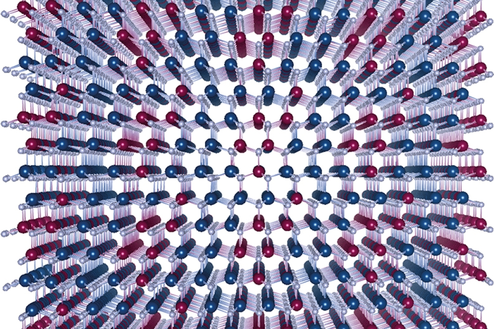
Main image: Atomic structure of an InGaN alloy

