WIN Semi announces linearity optimised GaN process
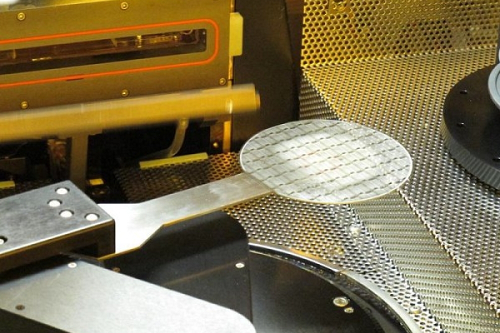
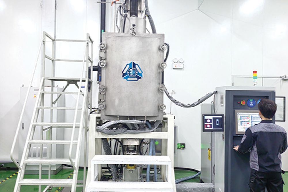
The Taiwanese compound semiconductor foundry WIN Semiconductors has launched a 0.12 μm gate-length depletion-mode (D-mode) GaN HEMT technology on SiC substrates.
Engineered for demanding high-power applications across K-Band to V-Band frequencies, the NP12-1B process is said to deliver industry leading high power front end solutions with exceptional linearity, ruggedness, and reliability for next-generation RF and microwave systems.
Target applications include high-power microwave and mmWave communication systems, radar systems, electronic warfare and avionics, wireless infrastructure, ultra-wideband and broadband systems, and test & measurement equipment.
The NP12-01B incorporates multiple transistor improvements providing a combination of high breakdown voltage, enhanced linearity, and robust operation in continuous wave (CW) high-compression scenarios.
WIN says that the technology’s advanced source-coupled field plate design ensures a typical gate-to-drain breakdown voltage of 120 V, supporting high power density and system reliability.
NP12-1B is available with the Enhanced Moisture Ruggedness option, which provides excellent humidity resistance for use in plastic packaging.
NP12-1B is supported by a complete Process Design Kit featuring both large-signal and small-signal models.
The NP12-1B will be available for high volume production in Q3 2025.