Mitel Unveils 40-Channel MUX/DEMUX Prototype
Prototypes of New Photonic Devices Demonstrate Order of Magnitude Improvement in Price/Performance for DWDM Devices
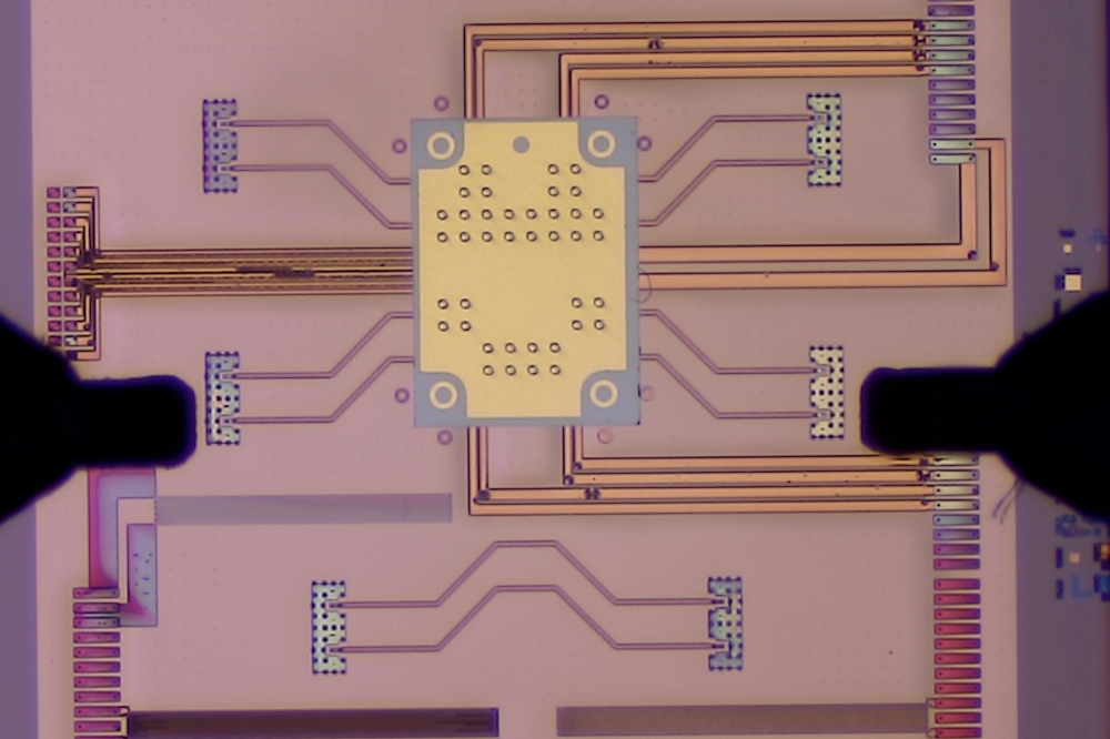
Mitel Semiconductor caused a stir last week by unveiling a 40-channel MUX/DEMUX prototype with 100 GHz channel spacing that will reduce the size and cost of DWDM modules. The device is based around an Echelle Grating etched in to glass (or silica) deposited on silicon.
OVERVIEW Mitel Semiconductor has produced working prototypes of photonic devices aimed at improving the price/performance ratio of Dense Wavelength Division Multiplexing (DWDM) by at least one order of magnitude. The technology is core to Mitel s strategy to support broadband connectivity within and between multi-service networks. The prototypes are based on an innovative process technology that allows more channels to be integrated into smaller devices, significantly reducing the cost of implementing DWDM in high-speed communications equipment.
Most commercially available MUX/DEMUX solutions are based on thin film filters, Bragg Gratings, and free space gratings, which are suitable for up to 16 channels. Since these technologies are expensive and very difficult to manufacture, the industry has moved to Arrayed Waveguide Gratings (AWG) for devices with up to 40 channels. However, higher numbers of channels using this approach are expensive to manufacture and the resulting chip size may be too large to be handled by conventional photolithographic techniques and equipment.
CORE TECHNOLOGY To overcome these limitations, Mitel employed a different form of grating known as an Echelle Grating, and tapped into its proven semiconductor fabrication expertise to develop a number of proprietary, patentable techniques. The result may lead to a higher-capacity, single-chip device based on standard semiconductor materials that dramatically alters the economics of high-speed optical communications.
The technology solves challenges associated with:
-- Material Deposition: depositing thick layers of glass (or silica) on a silicon base. Mitel is able to accurately control the material’s uniformity and thickness, which makes its refractive index – hence performance – predictable
-- Precision Etching: implementing an accurate Echelle grating. The challenge is to deliver high-quality optical multiplexing by ensuring that light reflects and is propagated with extreme precision.
-- Product Realization: qualifying the resultant devices and their physical packaging in an hermetic enclosure. The challenges are to ensure that the device s performance is not affected by the polarization of light, and to push the envelope in automation to obtain higher yields than competing alternatives.
LightRider™ FAMILY Mitel s optical multiplexer family of products based on this technology will be called LightRider*. Mitel expects to provide its lead customers with LightRider samples for evaluation by early next year.
The first device will be a 40-channel multiplexer/de-multiplexer (MUX/DEMUX) with 100GHz channel spacing that will reduce the size and cost of DWDM modules. The technology developed at Mitel’s facilities in Bromont Quebec, Canada has potential to reduce size by a factor 5X compared to alternative approaches. As a result, the family will be ideal for meeting increased bandwidth requirements at the core of high-speed network equipment
RESEARCH AND DEVELOPMENT This development program is another step in Mitel’s progress in photonics and optoelectronics. The company continues to explore new frontiers with research organizations and universities, and recently established the Mitel Photonics Fund at the University of Ottawa to foster advanced multidisciplinary research.
MARKET INFORMATION DWDM is a key technology for accommodating the exploding bandwidth requirements of the communications infrastructure. The technology allows more data over the existing infrastructure by multiplexing multiple wavelengths of light over a single fiber optic cable. The ability to increase bandwidth without incurring costs associated with installing additional cable is driving the substantial growth expected of this market over the next few years. This market for DWDM equipment serving Metropolitan Area Networks is currently forecast by Pioneer Consulting to grow from US $375 million today, to US $2.04 billion by 2004 (LLC report “Market opportunities for optical switching, routing and crossconnect in DWDM networks,” January 2000).
NOTABLE QUOTABLES Moving this technology to silicon instead of relying on more expensive and exotic materials holds significant promise for cheaper, more reliable devices that are essential for high-speed optical transmission. Mitel s approach will positively influence performance and cost limitations. - Dr. R. Normandin, Director General, Institute for Microstructural Sciences, National Research Council of Canada.
This is an example of what some people call disruptive technology. By being able to etch deep enough, smooth enough and vertical enough into silica, we have laid the foundation for dramatic improvements in the capacity, size and cost of these devices. - Moris Simson, Senior Vice President and Chief Technology and Marketing Officer, Mitel Corporation.
With a 40-channel multiplexing device, we believe our footprint per channel is five times smaller than competing alternatives. With this level of miniaturization, our approach provides unprecedented scalability leading to higher capacities, and reduces the need for expensive, highly specialized amplifiers in the network. Mitel’s current prototype conforms to the ITU-T grid with 100 GHz channel spacing. An 80-channel 50 GHz device is also in development. - Dr. John Miller, Director of Photonics, Mitel Semiconductor
ABOUT MITEL SEMICONDUCTOR Mitel Semiconductor specializes in connectivity solutions for the communications and medical industries with a product range that includes components for both wired and wireless networks; microelectronics for enabling the convergence of voice and data; optoelectronic devices for high-speed Internet systems; and applications-specific integrated circuits (ASICs) for medical applications such as pacemakers and hearing aids. For more information visit www.mitelsemi.com.
ADDITIONAL BACKGROUND INFORMATION Photo: A scanning electron micrograph illustrating Mitel’s precision etching can be viewed at www.mitel.com.
Press release: "Mitel Pushes the Boundaries of Optical Communications," August 10, 2000, can be accessed at www.mitel.com
CONTACTS Patti Dalby, Mitel Semiconductor, (613)592-2122 patti_dalby@mitelsemi.com Tiana Wiersma, BW&A, (503) 241-6183, tiana@bwpr.com
* LightRider is a Mitel Corporation registered trademark.
E-mail: tiana@bwpr.com
Web site: http://www.mitel.com


