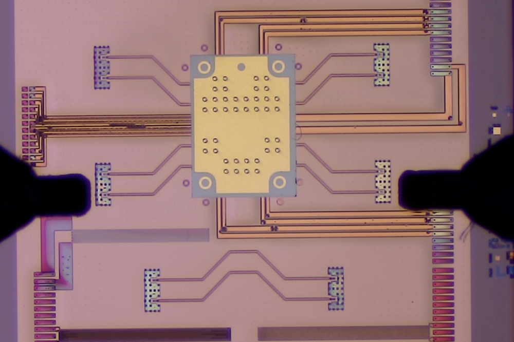
2-Inch Gallium Nitride Epitaxial Substrate Completed by Kyma Technologies
Source: Kyma Technologies
Research Triangle Park, NC. Kyma Technologies(TM), a developer and supplier of nitride substrates, has completed development of a 2-inch diameter, 50-micron thick epitaxial gallium nitride (GaN) layer, on a sapphire wafer, to be used as the core technology for a variety of applications within the optoelectronic, communications and semiconductor industries.
GaN substrates result in fewer processing steps and improved device quality for device manufacturers who rely on the wafers as core material for GaN-based wide bandgap semiconductor devices. In the future, devices based on GaN will mean reduced power consumption, brighter lights, longer device life and higher quality products for the public. Kyma will be shipping samples to device developers by the end of the year, with production quantities available in the first quarter of 2001.
About GaN Substrates
Until now, the typical epitaxy is 1-2 microns for sapphire-based GaN wafers. Since May 2000, Kyma has been moving rapidly to complete product development of a freestanding GaN substrate with the support of 2 Phase I Small Business Innovation Research (SBIR) contracts. Kyma s development of a sapphire-based GaN substrate marks a major milestone towards the completion of the company s freestanding, high purity GaN substrate.
Examples of GaN-based device applications that will be enhanced by the use of larger GaN substrates include short wavelength semiconductor lasers, high brightness visible and UV LED s, advanced RF communication components, solar blind UV photodetectors, high power semiconductor devices.
About Kyma Technologies
Founded in 1998 by Chief Scientific Officer Jerry Cuomo, PhD, and Mark Williams, Director of AlN Research and Development, Kyma Technologies is a spin-off from North Carolina State s Department of Materials, Science and Engineering and is a leading developer of nitride substrates. The company has received a series of STTR and SBIR contracts to fund various phases of nitride research, playing a pivotal role in bringing high-purity AlN and GaN to nitride device manufacturers reliant on high quality core materials. Since 1998, Kyma Technologies has expanded its development and manufacturing facilities to accommodate its rapid growth and is applying for additional contracts to support its research objectives, with a strong focus on gallium nitride as well as aluminum. To learn more about Kyma Technologies, please visit the company s Website at www.kymatech.com.
Contact: Ed Pupa of Kyma Technologies Tel: 919-789-8880 or Wendy Helmick Tel: 919-465-2062 for Kyma Technologies
Ed Pupa of Kyma TechnologiesTel: 919-789-8880
or Wendy Helmick
Tel: 919-465-2062 for Kyma Technologies
Web site: http://www.kymatech.com


