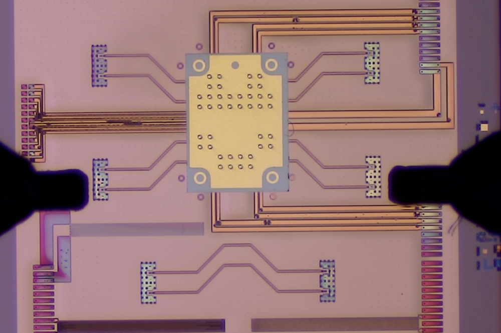
Nitronex Announces Industry's First GaN-Based Transistors on 4-inch Silicon Wafers
Source: Nitronex
Electron Mobility Exceeds 1600 cm2/Vs; Advancements Enabled By Company s
Proprietary PENDEO™ Processing
RALEIGH, N.C. Nitronex Corp., one of the first wireless components suppliers to focus
exclusively on GaN (gallium nitride), today announced it is producing the industry s first
GaN-based HEMTs (high electron mobility transistors) on low-cost, 4" silicon wafers. Until now,
industry efforts were limited to 2" wafers.
The company also announced it is consistently obtaining room temperature two-dimensional
electron gas mobilities exceeding 1600 cm2/Vs on GaN-based HEMTs deposited on 4" silicon.
This is one of the highest electron mobilities ever reported for GaN transistors, demonstrating
the high quality of Nitronex s material.
"These significant accomplishments will help make wireless GaN transistors a commercial
reality," said Bob Lynch, Nitronex Corp. s president and CEO. "This work is a direct result
of the unparalleled intellectual property that Nitronex has and continues to develop by focusing
exclusively on gallium nitride. By combining the performance benefits of GaN with the cost
advantages of large-area silicon substrates, Nitronex is poised to set the standard for high-power,
high-frequency power amplifiers."
The results reported today were achieved using Nitronex s proprietary MOCVD (metal organic
chemical vapor deposition) growth equipment and deposition process. The patent-pending
PENDEO processing developed by company engineers reduces GaN crystal defects by more
than 100,000 times relative to conventional growth techniques.
Nitronex also stated that DC and RF device measurements are exceeding expectations,
and the company anticipates announcing initial results and product studies in early second quarter 2001.
Added Warren Weeks, Nitronex s director of materials engineering, "The lack of commercially
available OEM solutions for growth of GaN on large-area substrates necessitated our internal
drive to develop large-area, MOCVD systems. The Nitronex platforms are working better than
expected and are the keys to the great results announced today."
About Nitronex Nitronex s GaN (gallium nitride) technology is helping create the infrastructure necessary for
emerging high-bandwidth wireless communications. The company s proprietary PENDEO
processing is unique in its ability to reduce GaN crystal defects by more than 100,000 times relative
to conventional growth techniques. Additional information on Nitronex is available at www.nitronex.com.
For more information, please contact: Jason L. Dunn Porter Novelli Convergence Group Phone: 919-834-1213 jason.dunn@pnicg.com
Bob Lynch Nitronex Corp. 919-807-9100 bob_lynch@nitronex.com
Jason L. Dunn
Porter Novelli Convergence Group
Phone: 919-834-1213
jason.dunn@pnicg.com
Bob Lynch
Nitronex Corp.
919-807-9100
bob_lynch@nitronex.com
E-mail: bob_lynch@nitronex.com
Web site: http://www.nitronix.com


