IBM Announces Worlds Fastest Silicon-Based Transistor
New Chip Technology Breaks Speed Barrier at Ultra-Low Power
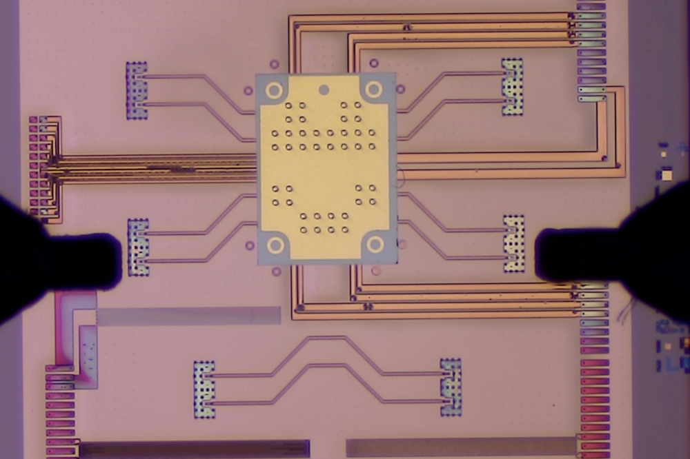
EAST FISHKILL, N.Y. IBM today announced it has built the world s fastest silicon-based transistor, a basic building block used to make microchips. I BM expects the new transistor will drive communications chips to speeds of 100GHz within two years -- five times faster and four years sooner than recently-announced competitive approaches.
The transistor uses a modified design and IBM s proven silicon germanium (SiGe) technology to reach speeds of 210 GigaHertz (GHz) while drawing just a milliamp of electrical current. This represents an 80 percent performance improvement and a 50 percent reduction in power consumption over current designs.
Just as aircraft were once believed incapable of breaking an imaginary sound barrier , silicon-based transistors were once thought incapable of breaking a 200GHz speed barrier, said Bernard Meyerson, IBM Fellow and vice president, IBM Communications Research and Development Center. Makers of high performance electronics like networking gear are no longer forced to use chips made of exotic and expensive materials to reach these speeds. Silicon s future is safe as the preferred medium for chip-making.
Top-tier communications equipment makers are already working with the new IBM technology to help build faster, more efficient products to increase the speed of today s networks.
AMCC has proven that IBM s current SiGe process can achieve the critical speeds necessary for high-speed next generation optical networks, said Oswin Schreiber, senior product marketing manager, Applied Micro Circuits Corporation. ``We believe that IBM s next generation of SiGe can enable customers like AMCC to deliver devices that perform at even higher data rates to meet future networking requirements.
Transistor speeds are largely determined by how quickly electricity passes through them. This is dependent on the material the transistor is made of and the distance electricity must travel through it. Standard transistors are made of ordinary silicon. In 1989, IBM introduced an improvement to the basic silicon material by adding germanium to greatly speed the electrical flow, improving performance and reducing power consumption. With this latest achievement, IBM is combining the use of the SiGe material with an improved transistor design that shortens the electrical path to speed up the device.
In standard transistors, electricity travels horizontally, so shortening the path requires that the transistor be made thinner -- an increasingly difficult task with diminishing returns using today s chip manufacturing techniques. The IBM SiGe device is called a ``heterojunction bipolar transistor (HBT), an alternate transistor design in which electrical flow is vertical. In IBM s SiGe manufacturing process, the height of the transistor is more easily reduced by thinning the SiGe layer, shortening the path of electrical flow and improving performance.
This announcement represents a new plateau for SiGe. More importantly, it opens the door to new levels of performance, particularly in the never-ending race to improve networking gear to handle the growing needs of the Internet and e-business. An added advantage of IBM s SiGe technology is that SiGe chips can be built on existing manufacturing lines, which is critical in allowing the technology to be introduced rapidly and at minimal cost. This has expanded the use of SiGe technology for extending functions and battery life in cellular phones and other wireless communications products as well.
This advancement in SiGe technology is the latest in a string of chip materials improvements from IBM, continuing the technology leadership established with IBM firsts in the use of copper to replace aluminum wires, improved low-k insulation between wires and increased transistor performance through silicon-on-insulator (SOI) and strained silicon technologies. IBM is currently working with dozens of communications companies to incorporate SiGe into an array of products, using state-of-the-art IBM design centers in Waltham, MA, East Fishkill, N.Y. and Encinitas, Calif. in the U.S., as well as in LaGaude, France.
Images of this new breakthrough can be found at: http://www.chips.ibm.com/news/2001/0625_fastimages.html
More information on IBM s related semiconductor breakthroughs can be found at: http://www.chips.ibm.com/bluelogic/showcase/
About IBM
IBM Microelectronics is a key contributor to IBM s role as the world s premier information technology supplier. IBM Microelectronics develops, manufactures and markets state-of-the-art semiconductor and interconnect technologies, products and services. IBM makes chips for a wide range of devices from the world s most powerful computers to the smallest cell phones. Its superior integrated solutions can be found in many of the world s best-known electronic brands. More information about IBM Microelectronics can be found at: www.chips.ibm.com.
Contact:
IBM Microelectronics
Michael Loughran 845/892-5463
mloughra@us.ibm.com
Michael Loughran 845/892-5463
mloughra@us.ibm.com
E-mail: mloughra@us.ibm.com
Web site: http://www.chips.ibm.com


