Technical Insight
Ge substrates, metamorphic HEMTs and hybrid integration (Microelectronic Devices)
Raf Vandersmissen discusses the merits of different HEMT technologies for millimeter-wave devices and outlines IMEC's integration schemes for GaAs and Ge metamorphic HEMTs.
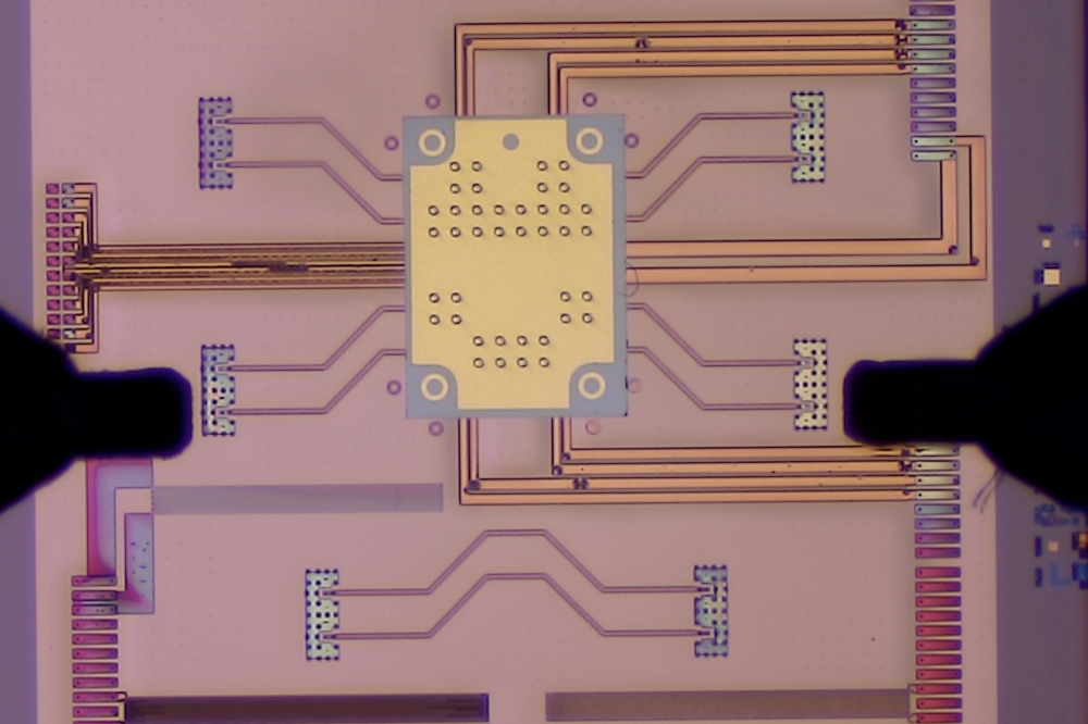
In the last decade the number of applications in the millimeter-wave range has grown tremendously. Critical to this growth has been the development of low-cost MMICs, or hybrid ICs, operating in the Q-band at 40 GHz and the W-band at 94 GHz. The latter frequency is suited to applications such as the high-resolution radars used in airport surveillance. Another emerging millimeter-wave market lies in the automotive industry for GPS navigation systems and collision-avoidance radars that work over a 100200 m range at 77 GHz. In the case of optical networks, the transistors must provide ft and fmax values of more than four times the bit rate in order to achieve the required switching speeds and system margins. Thus, current optical systems operating at 10 Gbit/s require GaAs HEMT or HBT technology with a cut-off frequency (ft) of at least 40 GHz. Moreover, in these optical networks there is a shift away from bare dies towards modules containing a photodetector and TIA on the receiver side, or a laser and modulator on the transmitter side. Such integration can be achieved either in InP technology or by using hybrid schemes such as the multichip module approach developed at IMEC to allow the cost-effective integration of different types of components. In this article we will compare millimeter-wave MMICs based on InP with metamorphic HEMTs (MHEMTs) employing GaAs and germanium substrates, and we will outline IMEC s recently introduced hybrid integration scheme that would enable active devices, such as MHEMTs, to be composited with passive components. Substrate economics MHEMTs grown on GaAs substrates have recently demonstrated a performance level close to that obtained from HEMTs grown lattice-matched to InP substrates. Improvements in backside processing and the availability of 6 inch GaAs substrates will probably induce metamorphic growth as an attractive alternative to InP HEMTs (Van der Zanden et al.). Further to this, the economic advantages of alternative substrates, such as germanium, which is around 50% less expensive than GaAs, can extend the price advantage even further compared with InP HEMTs. The use of germanium also offers a way to avoid prices for materials spiraling due to the reputed gallium shortage. Germanium is available in diameters of up to 8 inches and has a lower environmental impact than GaAs. The availability of large-area germanium wafers also lends itself to a hybrid integration approach for the low-cost packaging of MHEMT devices. IMEC s multichip module-dielectric, or MCM-D, technique employs a multilayered interconnection technology consisting of a glass substrate with alternating dielectric and metal layers on top. A spin-on low-k dielectric polymer layer is used in the integration scheme to attach the components. In this hybrid substrate, microwave passive components are embedded together with thinned active die, such as MHEMTs in a low-cost process described later in this article. MHEMT device geometry A typical MBE-grown metamorphic HEMT on a GaAs substrate is shown in . The 4% lattice mismatch between a GaAs substrate and the InGaAs channel can be overcome by using a GaAs nucleation layer and a 1 m InAlAs metamorphic buffer, which grades from AlAs to In0.57Al0.43As. A 100 nm reverse grade towards In0.52Al0.48As is then added to improve further the crystalline quality of the subsequent top layers. The heterostructure consists of a buffer, a channel layer in between two spacers (which ensures donor-electron separation), two silicon delta-doped InAlAs spacers, and a Schottky layer and cap (Behet et al.). At room temperature, this GaAs-based double delta-doped heterostructure has a low-field mobility of 6.85 103 cm2/Vs, an electron density of 5.7 1012 cm2 and a square resistance of 159 O. Similar results to these have been measured from devices grown on germanium substrates. IMEC s MHEMTs are fabricated with the same process used for the production of InP HEMTs. This process consists of four ultraviolet-lithography steps (mesa isolation,ohmic metal, contact metal and passivation) and one e-beam lithography step to define the T-shaped gate. InP HEMTs vs metamorphic HEMTs This , compares the DC and RF results of MHEMT devices (0.2 m gate length) grown on GaAs and germanium substrates with those from lattice-matched HEMTs on InP. The results are obtained on devices processed with a mask set that is not optimized for RF applications (i.e. they exhibit large pad capacitance). Only extrinsic values are given to make a direct comparison between different layer structures. The germanium MHEMT devices show DC performance parameters that are comparable to the GaAs circuits, and are even comparable to InP HEMTs. However, a large discrepancy is revealed in the much lower RF performance (ft = 45 GHz and fmax = 68 GHz), which is due to the limited resistivity of the germanium substrate. Devices grown on GaAs and InP achieve much higher RF performance because both types of substrate are semi-insulating. Several co-planar high-gain MMIC amplifiers have been fabricated using MHEMT epilayer structures. Two narrowband high-gain circuits, originally designed to be processed using InP-based circuits, were realized in co-planar waveguide technology. At 40.5 GHz, the gain reaches a maximum of 17.5 dB and is complemented by an excellent input and output matching of 19 and 27 dB respectively. The corresponding values for the original InP HEMT include a maximum gain of 17 dB and input and output matching of 15 and 20 dB respectively. However, to compete with InP, the GaAs MHEMT must be able to demonstrate its abilities at frequencies of more than 80 GHz (W-band). shows an SEM photograph of a co-planar W-band amplifier. The layout comprises transmission lines, MIM capacitors and resistors. The original InP circuit demonstrates a gain of 12.4 dB at 94 GHz, whereas the GaAs MMIC yields a maximum gain of 10.5 dB at 84 GHz. The shift in frequency can be attributed to a lower output conductance due to the high bandgap material (InAlAs) in the metamorphic buffer. An adjustment of the matching network in the GaAs MMIC is required to obtain the maximum gain at 94 GHz. Hybrid integration of Ge MHEMTs In the case of germanium MHEMTs, the conductive nature of the substrate makes such devices unsuitable for millimeter-wave applications. The substrate, having served its purpose as a platform for growth, is removed and the MHEMT device is transferred to a hybrid substrate for further integration (). Prior to the removal of the substrate, the wafer is diced and a chip containing one MHEMT transistor mounted on a 6 inch glass substrate (with the active side facing the glass) in a 3 m thick spin-coated polymer layer of benzocyclobutene (BCB). As a low-k dielectric polymer with a high glass transition temperature (of up to 350 C), BCB is very suitable for RF integration and microelectronics. This polymer film protects the front face of the chip. The germanium substrate is removed by reactive ion etching in a mixture of CF4 and O2. The GaAs buffer is then selectively etched, and the buffer layer is removed from regions surrounding the active area using lithography and a non-selective etch of phosphoric acid. This step reveals the metal contacts of the 2 m thick devices, which are contacted by probe needles from the back-side. The latter process, which contacts the metal directly, is very straightforward and designed to realize amplifier circuits in the MCM-D technology. Moreover, to circumvent planarization problems in subsequent MCM-D processing steps, the total thickness of the devices is kept below 5 m. This requirement is easily maintained due to the removal of the substrate. Performance of germanium MHEMTs shows an optical micrograph of a thin-film MHEMT following substrate removal on a glass MCM-D platform. The image is obtained from the back-side to reveal the contact metal and active area. Measurements of hybrid glass germanium MHEMTs reveals only a slightly reduced DC performance the drain-to-source current (Ids) still reaches a value of just over 600 mA/mm. However, the maximum transconductance (gm) has dropped to 675 mS/mm. This degradation is attributed to heat generated in the thin active area of the devices. On the other hand, the RF performance recovers considerably. With an ft of 70 GHz and an fmax equal to 120 GHz, the germanium device is approaching the performance of GaAs MHEMTs. These extrinsic results confirm that the conductivity of the substrate is responsible for most of the degraded performance in germanium MHEMTs, and that this problem can be largely overcome by removing the substrate. Other technologies and the future The fastest transistor ever built is an InP HEMT, and for almost a decade such devices have offered an optimum combination of high-gain, low-noise and high-speed performance for three-terminal devices. On the other hand, GaAs MHEMT circuits have similar layer structures, with DC and RF performances approaching 90% of those for InP devices, and they are much cheaper. This makes metamorphic MMICs, especially in the W-band, strong competition for InP MMICs in cost-driven mass-market applications. At IMEC we have also demonstrated the potential of reducing costs even more through the hybrid integration of MHEMTs on germanium substrates. After substrate removal and hybrid integration, such devices exhibit RF results comparable to those of their GaAs MHEMT counterparts. Hybrid integration is often the only feasible solution because of the heterogeneity of components and the complexity of certain RF systems. Compared with hybrid integration using flip-chip with bumps, IMEC s approach results in smaller parasitic capacitance and allows for stacked three-dimensional circuits. MCM-D integration is well suited to RF applications beyond 50 GHz due to its high definition and the possibility of integrating resistive and capacitive layers. However, while the minimal thickness is advantageous, it limits applications to low-power circuits. The MCM-D approach will also be feasible for future fiber-optic components, particularly as the evolution to higher levels of integration will lead to transponder modules, such as lasers, MUX and optical amplifier functions on a common glass substrate (Lebby). However, InP will probably be the material of choice for the development of very-high-bit-rate components in optical networks at 40 Gbit/s and above. This material offers the potential for ft values in excess of 200 GHz and the ability to integrate a sufficient number of transistors along with lasers, detectors and modulators (Deyhimy). However, because the hybrid integration approach developed at IMEC is a generic one, work in the future will focus on integrating thin-film GaN HEMTs on AlN substrates for power applications. l Further reading Behet et al. 1998 Appl. Phys. Lett. 73 2760. Deyhimy 2001 Compound Semiconductor July 77. Lebby 2001 ibid. 81. Van der Zanden et al. 2000 GaAs Mantech Digest 229.


