WJ to close GaAs facility in restructuring move
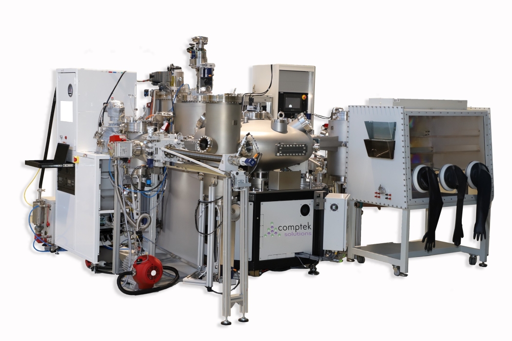
WJ Communications, the maker of RFICs for wireless infrastructure applications, is to close its GaAs wafer manufacturing facility early next year.
The San Jose, CA, firm, which acquired the GaAs fab in nearby Fremont when it bought EiC Corporation s wireless infrastructure business in June 2004 (see related story), has decided to become fabless in a move that could reduce annual costs by up to $5 million.
WJ has been working with Global Communication Semiconductors (GCS), the pure-play compound wafer foundry company, since March 2006. GCS has been acting as a second-source for WJ to provide InGaP HBT and GaAs material, but will now become its main supplier.
WJ's CEO Bruce Diamond said of the new strategy: "As a result of our successful qualification and production ramp [with GCS], we have solidified a restructuring plan, resulting in the planned closure of our wafer manufacturing facility during the first quarter of 2007."
Closing the 4-inch GaAs fab will cost WJ an estimated $1.5 million, although some of that could be recouped through the sale of manufacturing equipment.
However, the leaner cost structure should ultimately benefit the company to the tune of $5 million per year.
WJ is following in the footsteps of former GaAs chip maker Mimix Broadband, which decided to become fabless earlier this year, as well as Hittite Microwave, the Chelmsford, MA, company that has proved how profitable this business model can be (see related story).
WJ has also reported improving sales, and posted a revenue of $12.7 million - up 57 per cent on last year - for the financial quarter that ended on October 1. It made a net loss of $1.2 million, suggesting that financial break-even ought to be possible after the GaAs facility has been closed.


