'All-GO-HEMT' to develop β-gallium oxide heterostructures
A €2 million German-funded project called All-GO-HEMT aims to increase in efficiency in power electronics and make a significant contribution to sustainable energy generation.
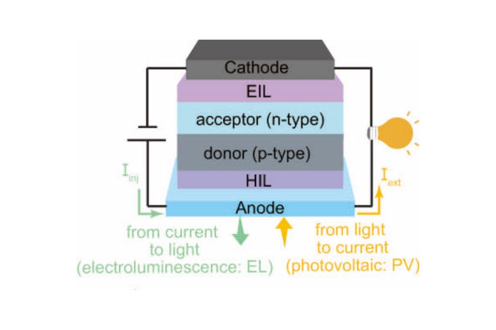
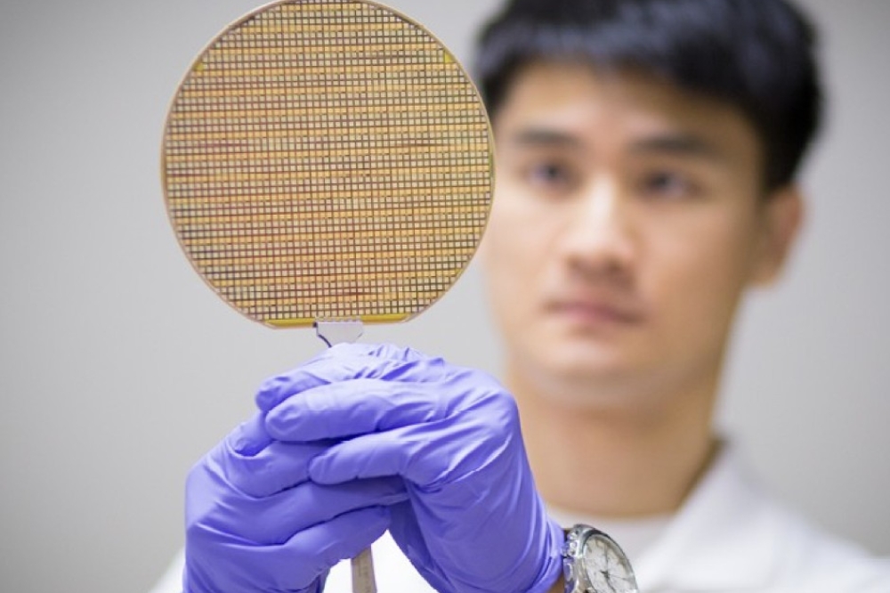
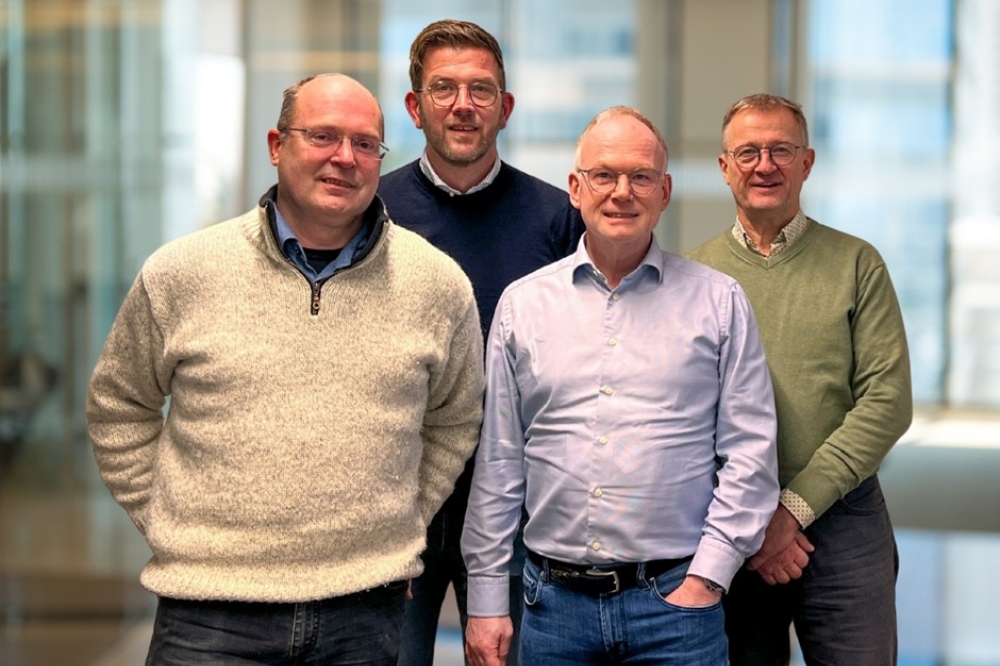
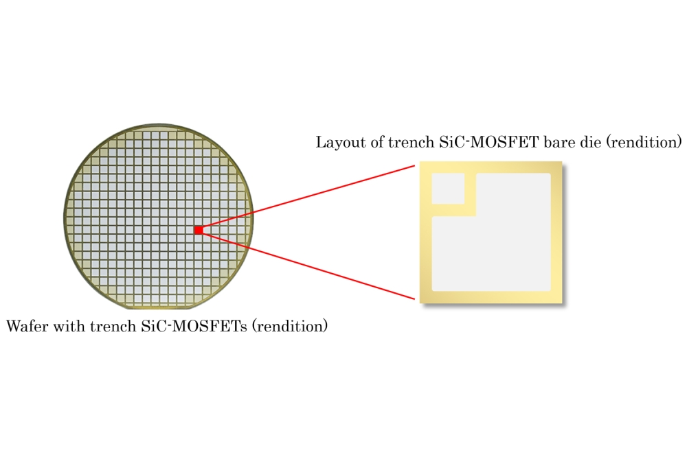
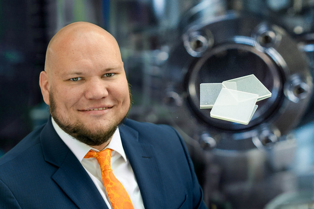
Led by Andreas Fiedler (pictured above) of the Leibniz-Institut für Kristallzüchtung (IKZ), the project aims to develop modulation-doped β-(AlₓGa₁₋ₓ)₂O₃/Ga₂O₃ heterostructures that exhibit high electron mobility.
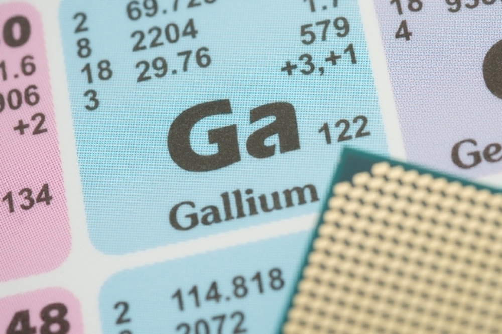
Compared to established materials such as silicon, GaN and SiC, Ga2O3 offers potential for increasing efficiency that has not yet been fully exploited. “We believe that the development of more efficient materials can make a significant contribution to the energy transition and enable the industry to successfully master the challenges of the future,” explains Fiedler.
Even though power electronics based on Ga2O3 promise to be more efficient, the material is inferior to established materials in terms of charge carrier mobility. “Gallium oxide behaves to the established materials in the same way as ten metres of dirt road to one kilometre of freeway. Due to the shorter distance, your car consumes less, and despite the lower speed, you reach your destination faster - all thanks to a more compact design,” explains Fiedler.
The central aim of the project is to overcome the material limitation of Ga2O3 in terms of charge carrier mobility with the help of the innovative design of an aluminium-alloyed heterostructure and thus eliminate this disadvantage.
Fiedler emphasises: “We are convinced that the efficiency of power electronics can be significantly increased through a combination of a more compact design and higher charge carrier mobility in our newly developed materials.”
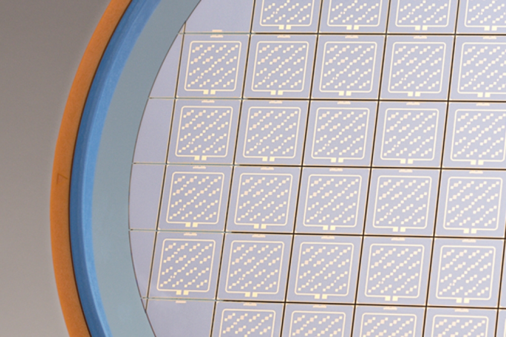
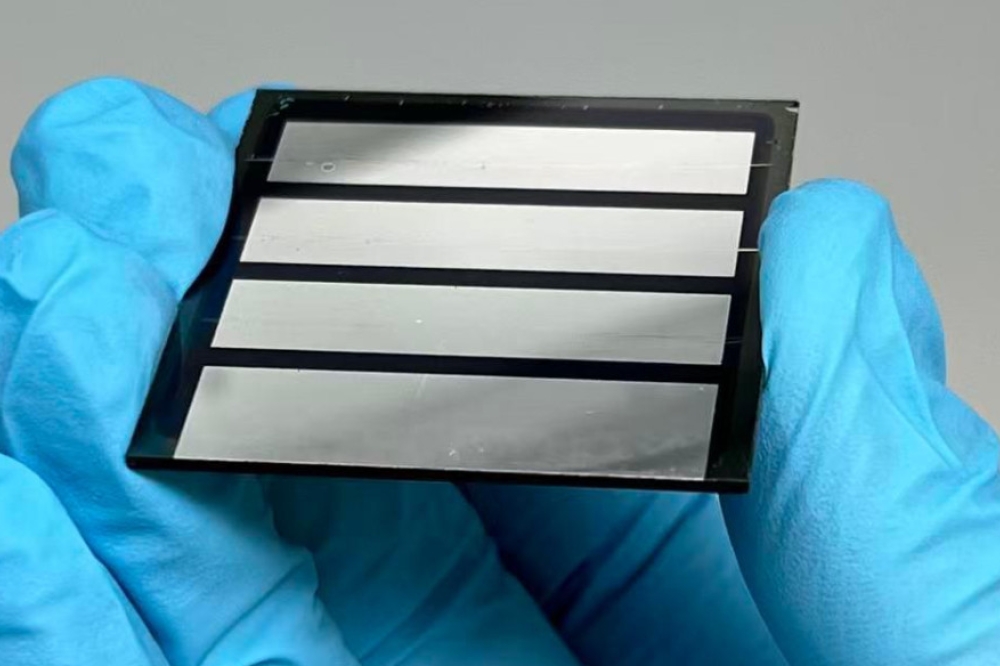
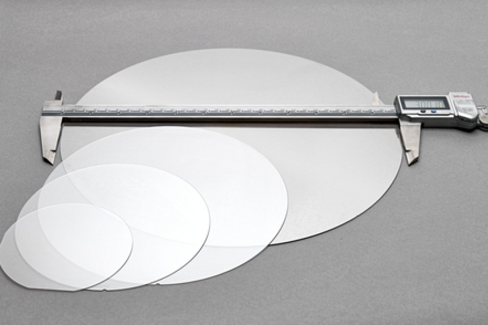
Another goal of All-GO-HEMT is to create a reliable material basis of Ga2O3 and the newly developed alloy with aluminum of the highest crystalline quality for research and industry. This basis is necessary because the development of high-performance devices with compact design and optimised manufacturing processes is currently limited by the insufficient availability of high-quality material.
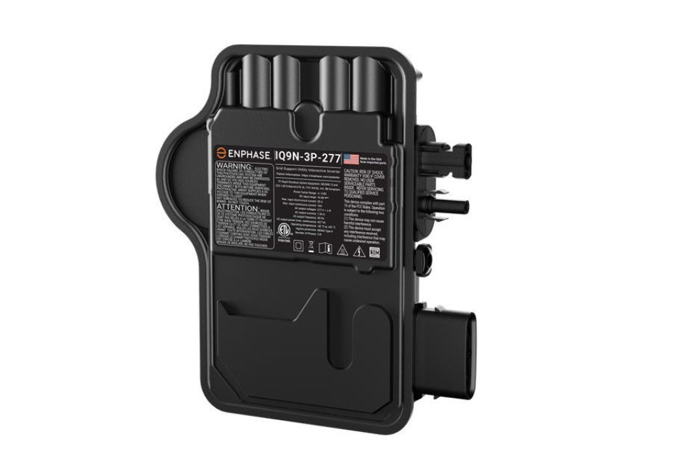
The project partner Ferdinand-Braun Institut (FBH) will use this material basis to develop new prototypes for power electronic devices. These prototypes will then be tested by ZF Friedrichshafen AG, the industrial mentor, for their suitability for industrial application. In addition, the entire value chain, from crystal growth to the finished device, will be analysed by the industrial mentors Aixtron SE and Siltronic AG in order to quantify and evaluate the economic and ecological benefits of this technology at an early stage.