
Akhan Semiconductor to scale diamond electronics for market
With the manufacture of 300mm diamond CMOS wafers demonstrated, Akhan is set to bring unprecedented power densities to RF power devices, reports Rebecca Pool.
In a very short space of time, US-based Akhan Semiconductor, has signalled a clear intent to massively scale up production of its synthetic, lab-grown electronics-grade diamond materials. In late June, former president of Intel Americas, Tom Lacey, joined the company board as chairman. The semiconductor executive has also spearheaded start-ups, mid-sized and larger public and private companies, and as he says: “Now is the time to unleash diamond's immense capability on chips, as well as optical and glass coatings.”
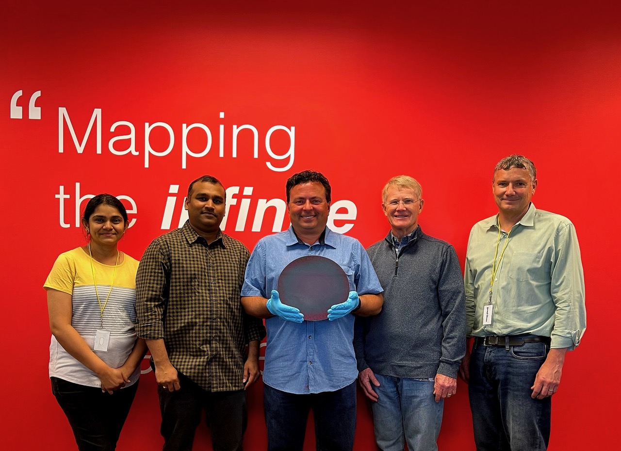
Then, only a few weeks later, Akhan revealed it had fabricated 300 mm diamond CMOS wafers at its production facility, northern Illinois Diamond Mine 1. As Adam Khan, company founder, puts it: “From a commercial standpoint, 300 mm is the standard, and we want to show that we have these processes that can form even the most advanced chips.”
“We've transitioned from laboratory innovations to repeatable and massively scaleable processes,” he adds. “With Tom, we're moving from an entrepreneurial phase to operational growth... We want to license our materials to fabs and end-customers worldwide so they can incorporate these into their chip designs.”
Early days
Khan founded Akhan Semiconductor back in late 2012, confident that diamond could deliver excellent display glass properties for smartphone screens and optical performance for mirrors and lenses. He was also certain that diamond semiconductors could replace silicon devices and outperform wide bandgap materials including GaN and SiC.
Partnering with Argonne National Laboratory, Akhan obtained exclusive rights to license the centre's diamond carbon vapour deposition technology, which enabled nanocrystalline diamond film deposition onto wafer materials at temperatures as low as 400ºC. Combined with Akhan's co-doping method - in which devices are doped with phosphorus and nitrogen, and then doped with boron or lithium to engineer atomic distribution - the pairing looked set to fulfil Khan's hopes.
As Argonne Materials Scientist, Anirudha Sumant, said at the time: “This licensing agreement gives us the impact of a one-two punch, in which we combine Akhan's novel process to achieve efficient n-type doping in diamond with Argonne’s low-temperature diamond deposition technology... This will break barriers that restricted the use of diamond thin films in the semiconductor industry to only p-type doping.”
Fast forward to today and this approach has been a success. Akhan has filed more than 40 patents worldwide, supplied its technology to Lockheed Martin, an unnamed smartphone OEM and other key industry players, and has now demonstrated the manufacture of 300 mm CMOS diamond wafers.
According to Khan: “We've done this using hot filament CVD [widely used to deposit diamond films] and get exceptionally high yield... the rejection rate has been less than 10% with wafers being rejected due to edge-to-edge film variability rather than tolerance.”
“This is a robust, scaleable process but 300mm is not our maximum size – we can grow diamond on panels even larger than this,” he adds.

Adam Khan, Founder of Akhan Semiconductor.
The company works with an impressive range of substrates, including silicon, glass, fused silica, sapphire, SiC, GaN and other crystalline semiconductor materials, and refractory metals. Devices for automotive applications are being fabricated on either silicon or SiC substrates.
“We have patents and 'trade secret' processes for each material, including how we prepare the material, growth conditions and post-processing,” says Khan. “The seed material and chemicals used to functionalise this vary by material type, and also by material thickness, roughness or finish.”
As the Akhan founder also points out, the material's crystal size is altered depending on the applications - for example, a large grain polycrystalline material enhances carrier mobility for high power, high frequency applications. “We haven't seen the need to develop single crystal [materials] for the applications we've pursued as what we are seeing is already so much better than SiC and GaN,” he says.
Indeed, along the way, Khan and colleagues have been tracking SiC and GaN developments in the RF power sector, and fabricating MOSFETs, MESFETs, bipolar and CMOS structures that bring unprecedented power densities to this application.
“We demonstrated a working diode back in 2013 and are currently deploying technologies with Lockheed Martin... [this includes] a joint effort with our diamond-based electronics and optics on their F-35 platform,” highlights Khan.
Performance-wise, Khan says power density of his diamond semiconductors beats that of GaN and SiC, exceeding 40 W/mm, while carrier mobility hits many hundreds of cm2/Vs. Patent detail indicates a monolithically integrated diamond semiconductor to have conduction electrons with a mobility exceeding 770 cm2/Vs at 300K. “We know it's quite fast in terms of switching,” says Khan.
Khan also reckons his devices are cheaper, per dollar/cm2, than the GaN and SiC equivalent. “We only use a very thin layer of diamond – just enough for the active layer,” he says. “Then the substrate cost is just silicon – which is cheaper than GaN and SiC.”
So what now for Akhan Semiconductor and its diamond electronics? The company has historically delivered materials for aerospace and defence applications, but is now preparing to launch products into automotive applications.
“We've focused on this since 2012... we're ready to start licensing our first technologies, including power inverters, and will have them in the [automotive] market by the 2021 time-frame,” says Khan. “Once the revenues are there for the automotive side, I think consumer electronics will be next.”


