
Tektronix speeds up SiC and GaN validation time
WBG de-skew technique, and reverse recovery timing plots, make it easier for engineers to optimise designs
Test and measurement firm Tektronix has announced a new release of its Double Pulse Test solution (WBG-DPT), with the ability to provide automated, repeatable, and accurate measurements on wide bandgap devices such as SiC and GaN MOSFETs.
According to the company, designers of next-generation power converters will now be able to use the WBG-DPT solution to optimie their designs confidently and quickly.
With the ability to run on Tektronix 4, 5 and 6 Series MSO oscilloscopes, integrating into the measurement system of the oscilloscopes, the WBG-DPT has an automatic WBG de-skew technique, and reverse recovery timing plots, making it easier for engineers to see reverse recovery details for multiple pulses overlaid on a single display.
Measurements are also designed to align with JEDEC and IEC standards for double pulse testing and diode reverse recovery.
“Tektronix customers are the designers of the next generation of cutting-edge power electronics technology, and their designs must be optimised to balance efficiency, size and reliability,” shares Daryl Ellis, Tektronix Mainstream Portfolio general manager.
“We are confident that the design of the Tektronix WBG-DPT Solution will allow for simplified debugging, repeatable measurements (per JEDEC and IEC standards) and a faster learning curve. Test automation reduces test times and retesting errors, ensuring our customers meet their project timelines and time to market plans.”
Masashi Nogawa, staff systems engineer at Qorvo said: “The WBG-DPT software provides instantaneous measurements of key parameters, like EON, EOFF, and QRR when performing double-pulse tests.
“The software makes the power waveform and markers showing the integration ranges used to calculate the energy losses immediately visible. This is an excellent alternative to exporting waveform data into Excel spreadsheets for processing.”
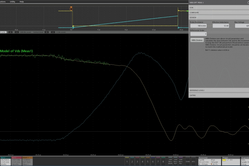
To achieve meaningful energy loss measurements, designers must correct for delays introduced by test fixtures and probes. The traditional technique for aligning drain-to-source- voltage (VDS) and drain current (ID) measurements requires rewiring the test setup and careful pretest measurements.
The WBG-DPT's WBG deskew technique eliminates the need for rewiring and may even be performed after double pulse measurements have been taken. To simulate the effects of delays in the test setup, the software generates an alignment waveform. The engineer adjusts a few settings to match the alignment waveform with the measured waveform, as the software corrects any differences in delays. This new process reduces the deskew time from an hour or more to just 5 to 10 minutes.


