
European team integrates GaSb lasers into PIC chips
Approach relies on Si-PIC design and fabrication, III-V material deposition, and laser fabrication
In a new paper published in Light Science & Applications, a team of scientists from France, Italy and Ireland, led by Eric Tournié from the University of Montpellier (France), claims to have unlocked the efficient integration of semiconductor lasers onto silicon photonics chips and light coupling into passive photonic devices.
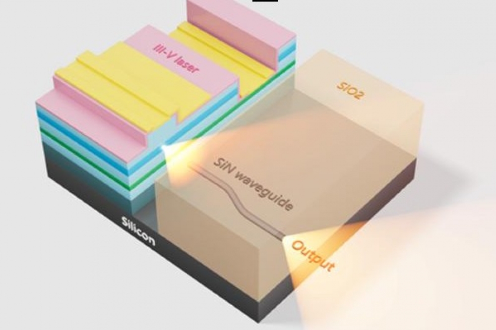
Their approach relied on Si-PIC design and fabrication, III-V material deposition, and laser fabrication. For this proof-of-concept, the PIC was made of transparent, S-shaped, SiN waveguides embedded in a SiO2 matrix. The SiO2/SiN/SiO2 stack was etched away in recessed areas to open silicon windows for the deposition of the III-V material.
GaSb was used as the III-V material because it can emit in the whole mid-infrared wavelength range, where many gases have their fingerprint absorption lines. Molecular-beam epitaxy was used to grow the semiconductor layer stack. The scientists had previously shown that this technique allows removing a special defect that usually occurs at the Si/III-V interface and kills the devices. Further, MBE allows to precisely align the laser part that emit light with the SiN waveguides.
Finally, a microelectronics process was used to create diode lasers from the epitaxial layer stack. At this stage high quality mirrors must be created through plasma etching in order to achieve laser emission. In spite of the process complexity, the performance of these integrated diode lasers were similar to those of diode lasers grown on their native GaSb substrate. Further, the laser light was coupled into the waveguides, with a coupling efficiency in line with theoretical calculations.
The scientists summarised the work as follows:
“The different challenges (PIC fabrication and patterning, regrowth on a pattern PIC, etched-facet laser processing in recessed areas, etc.) due to the particular architecture of the final devices were all overcome to demonstrate laser emission and light coupling into passive waveguides, with a coupling efficiency in line with theoretical calculations”.
“Although demonstrated with mid-infrared diode lasers targeting gas sensing applications, this approach can be applied to any semiconductor materials system. In addition, it can be scaled up to any Si-wafer size up to at least 300 mm diameter, epitaxial reactors being available.”
“The reported method and technique will open new avenues for future silicon photonics integrated circuits. They solve a longstanding problem, and lay the foundation for future low-cost, large-scale, fully-integrated photonic chips.”
Reference
'Unlocking the monolithic integration scenario: optical coupling between GaSb diode lasers epitaxially grown on patterned Si substrates and passive SiN waveguides' by Andres Remis et al; Light: Science & Applications volume 12, Article number: 150 (2023)


