Loading...
News Article

Aixtron launches compact platform for GaN devices

News

New G10-GaN cluster tool targets high-volume manufacturing of GaN-based power and RF devices

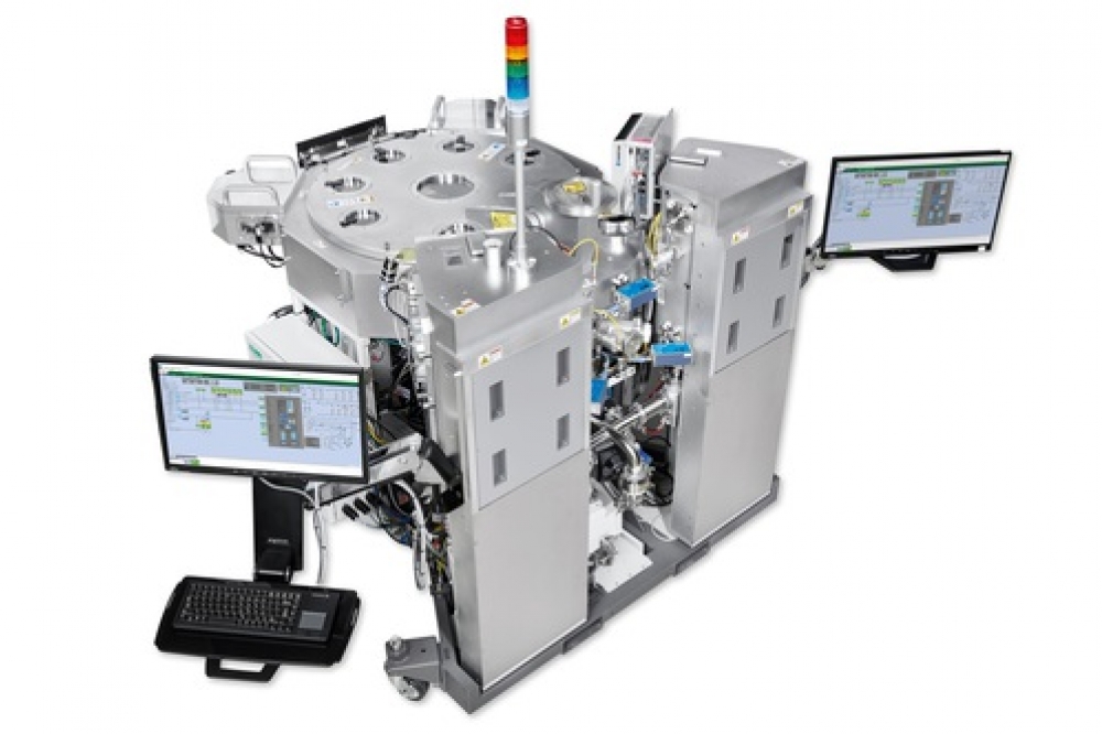
Deposition equipment specialist Aixtron SE has launched a new compact cluster solution for GaN based power and RF devices. The G10-GaN is currently being presented at SEMICON Taiwan in Taipei.

“We are proud that our new G10-GaN platform has already been qualified for volume production of GaN power devices by a leading US device manufacturer. The new platform delivers twice the productivity per cleanroom area than our previous product while enabling a new level of material uniformities, unlocking new levers of competitiveness for our customers,” says Felix Grawert, CEO and president of Aixtron SE.

Packed in a new, compact layout to take advantage of the smallest cleanroom space, the platform is said to feature novel reactor inlets, improving material uniformity by a factor of two for optimum device yields. On-board sensors are complemented by a new software suite and fingerprint solutions to ensure the system consistently delivers the same performance run after run, between maintenance for all process modules – extending the equipment uptime by more than 5 percent compared to the previous generation.

The cluster can be equipped with up to three process modules, delivering a capacity of 15x200 mm wafers thanks to Planetary batch reactor technology – enabling a 25 percent cost reduction per wafer compared to previous products, according to the company.

QD company Quantum Science expands into new facility
Innoscience files lawsuit against Infineon
Riber revenues up 5% to €41.2m
Forvia Hella to use CoolSiC for next generation charging
Photon Design to exhibit QD simulation tool
Ortel transfers CW laser fabrication to Canada
Luminus adds red and blue multi-mode Lasers
PseudolithIC raises $6M for heterogeneous chiplet tech
Mesa sidewall design improves HV DUV LEDs
IQE revenue to exceed expectations
'Game-changing' VCSEL system targets clinical imaging
German start-up secures finance for SiC processing tech
Macom signs preliminaries for CHIPS Act funding
IQE and Quintessent partner on QD lasers for AI
EU funds perovskite tandems for fuel-free space propulsion
EU to invest €3m in GeSi quantum project
Transforming the current density of AlN Schottky barrier diodes
Turbocharging the GaN MOSFET with a HfO₂ gate
Wolfspeed launches Gen 4 SiC MOSFET technology
Report predicts high growth for UK's North East
Element Six unveils Cu-diamond composite
SemiQ launches hi-rel 1700V SiC MOSFETs
Lynred to exhibit Eyesential SWIR sensor for machine vision
Thorlabs buys VCSEL firm Praevium Research
Advancing tuneable InP lasers on a heterogeneous platform
P-GaN gate HEMTs have record threshold voltage
Guerrilla RF releases GaN power amplifier dice
Narrow-linewidth DFB lasers now at 405 and 488nm
Researchers develop tech for future fast-charging stations
Vermont GaN Tech Hub awarded nearly $24M
Onsemi completes buy-out of Qorvo SiC JFET business
Quantum Science announces Innovate UK funding
×
Search the news archive

To close this popup you can press escape or click the close icon.
Logo
x
Logo
×
Register - Step 1

You may choose to subscribe to the Compound Semiconductor Magazine, the Compound Semiconductor Newsletter, or both. You may also request additional information if required, before submitting your application.


Please subscribe me to:


You chose the industry type of "Other"

Please enter the industry that you work in: