3D interconnects enable PV breakthrough
Researchers fabricate 3D interconnects on III-V/Ge triple-junction micro solar cells
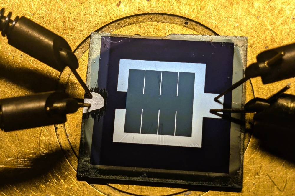
The University of Ottawa, together with national and international partners, has manufactured the first back-contact micrometric photovoltaic cells.
These III-V/Ge triple-junction micro solar cells are said to have significant advantages over conventional solar technologies, reducing electrode-induced shadowing by 95 percent and potentially lowering energy production costs by up to three times.
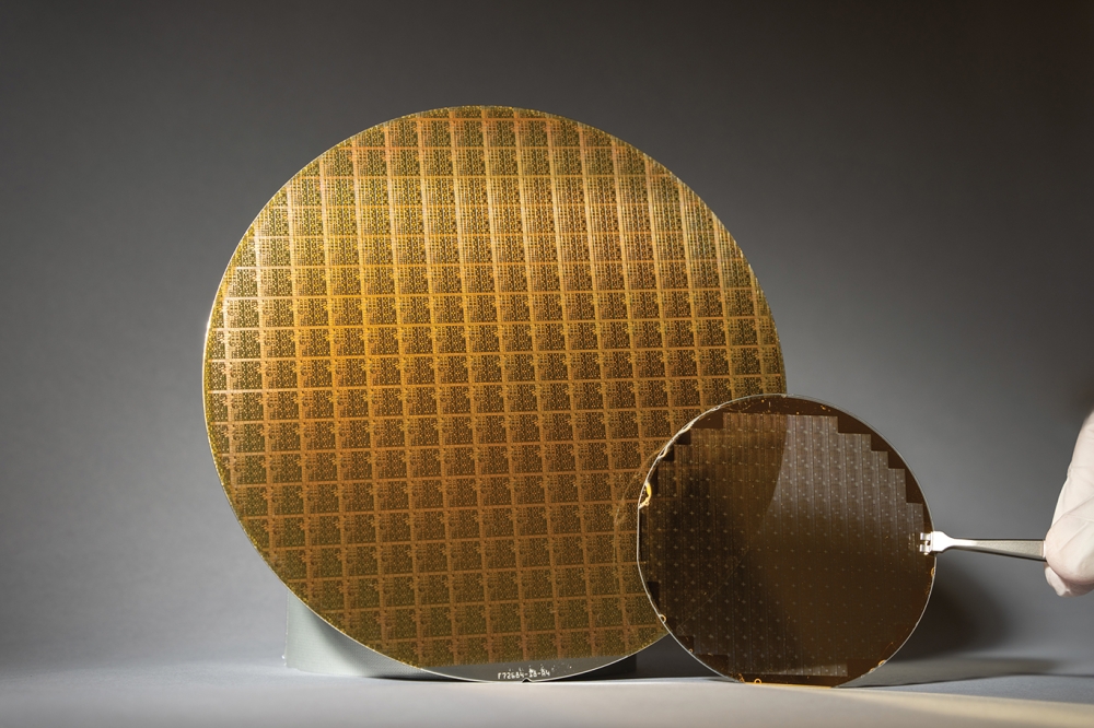
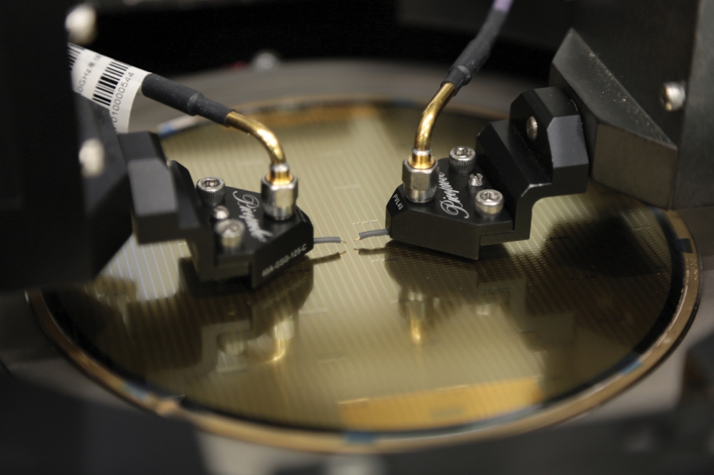
The team fabricated 3D interconnects on the multi-junction solar cells to increase power density and enable miniaturisation. They used methods including III-V heterostructure plasma etching, gold electrodeposition, and chemical-mechanical polishing to integrate through substrate vias to the heterostructure. Wafer bonding was used to handle 20-μm-thin III-V films.
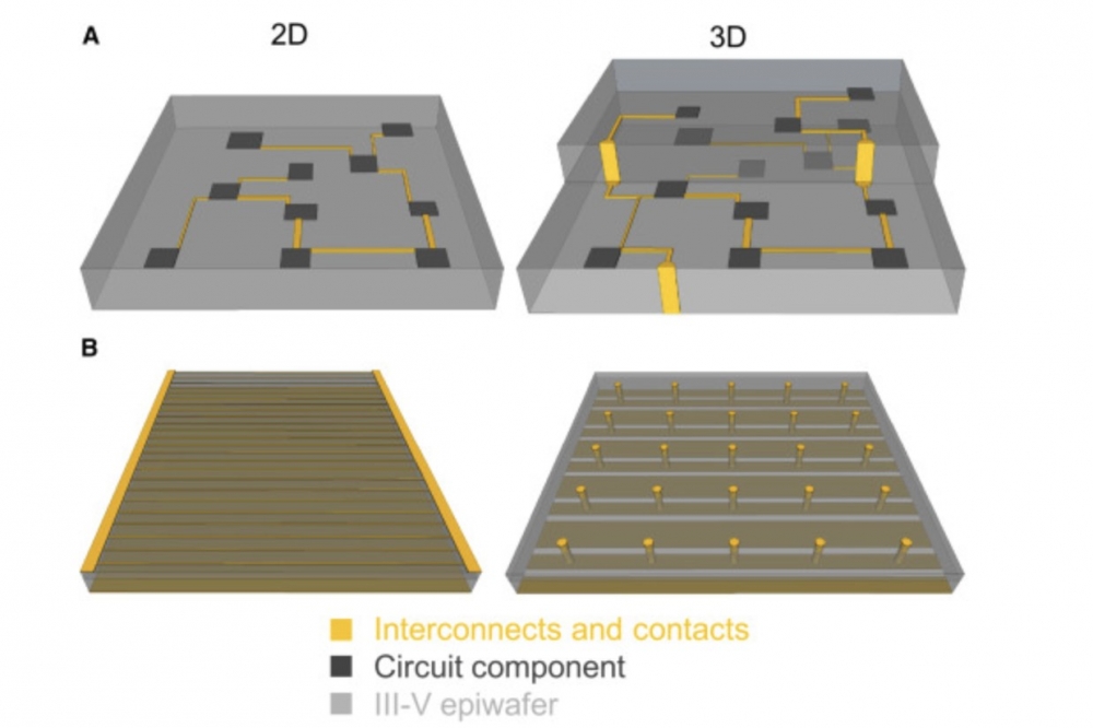
The picture above shows (A) schematics of a 2D electronic circuit on a III-V epiwafer and a 3D electronic circuit on two III-V epiwafers bonded together and interconnected with through substrate vias. (B) Thermophotovoltaic cell with 2D planar contacts and 3D interconnections using TSVs. Compared to miniaturised photonic power devices with 2D connections, the 3D interconnects achieve a six-fold increase in wafer area use to improve the power yield per wafer, according to the.
The research was led by Mathieu de Lafontaine, a postdoctoral researcher at the University of Ottawa and part-time physics professor; and Karin Hinzer, vice-dean, research, and University Research chair in Photonic Devices for Energy at the Faculty of Engineering.
“These micrometric photovoltaic cells have remarkable characteristics, including an extremely small size and significantly reduced shadowing. Those properties lend themselves to various applications, from densification of electronic devices to areas such as solar cells, lightweight nuclear batteries for space exploration and miniaturization of devices for telecommunications and the internet of things,” Hinzer says.
This initiative was funded by the Natural Sciences and Engineering Research Council of Canada, the Fonds de recherche du Québec Nature et technologies, the Horizon Europe Framework program, Prompt Québec and STACE Inc.
Reference
'3D Interconnects for III-V Semiconductor Heterostructures for Miniaturized Power Devices' by Mathieu de Lafontaine et al; Cell Reports Physical Science (2023)


