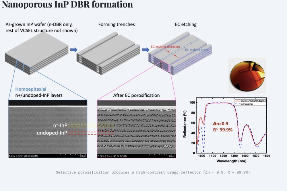
What goes on inside perovskite cells?

To improve the durability of tin perovskite, a method called Ruddlesden-Popper (RP) has been proposed that introduces large organic cations into tin perovskite crystals to form a 2D layered structure. This helps to suppress tin oxidation.
However, the internal state of this structure and the mechanism by which it improves performance is not clear.
Now scientists at the University of Tsukuba in Japan have used electron spin resonance to investigate an RP perovskite solar cell's internal state during operation from a microscopic perspective. Their work 'Operando spin observation elucidating performance-improvement mechanisms during operation of Ruddlesden-Popper Sn-based perovskite solar cells' appears in npj Flexible Electronics (2025).
Perovskite solar cells have a structure in which hole and electron transport layers surround a perovskite crystal. First, when no light was irradiated on the RP perovskite solar cell, the team found that holes diffused from the hole transport layer to the RP perovskite. This led to the formation of an energy barrier at the hole transport layer-RP tin perovskite interface, which suppressed the backflow of electrons and hence improved the performance.
Second, under sunlight irradiation, the researchers discovered that the electrons moved from the RP tin-based perovskite to the hole transport layer, attributable to the high-energy electrons produced by short-wavelength light, such as ultraviolet rays.
Further, the researchers found that this electron transfer increased the energy barrier at the hole transport layer-RP tin perovskite interface, further improving the device's efficiency.
The team say that understanding the mechanism behind the performance improvements during device operation is crucial for developing highly efficient, long-lasting solar cells and will contribute to future research developments.
Pictured above: a) Hole diffusion from the perovskite layer to the PEDOT:PSS layer under illumination and resulting electron barrier reduction. b) Electron diffusion from the perovskite layer to the PEDOT:PSS layer and resulting enhanced electron barrier. c) Enhanced electron barrier at the PEDOT:PSS/perovskite interface as a result of the two elemental processes. (CBM and VBM, respectively, represent the conduction band minimum and the valence band maximum).