IEDM: Multiple materials vie for RF success

Researchers at the recent International Electron Devices Meeting reported breakthroughs in RF devices made from many different materials.
BY RICHARD STEVENSON, EDITOR, CS MAGAZINE
Within the optoelectronic domain, the most suitable material for producing a particular device is pretty obvious. If you want to make a blue LED, use GaN; for a red variant, InGaP; and if you are to make a laser that’s targeting the low-absorption windows of a fibre, use InP. Selecting the best material for light emitters is easy, because the leading contender is identified by its bandgap.
The waters get a little murkier in the power electronics arena. From a theoretical standpoint, the best semiconductor is the one with the widest bandgap, so AlN. But that’s not the standout candidate when practical considerations are accounted for, such as the ease of doping, how hard it is to form an ohmic contact, and the availability and cost of suitable substrates.

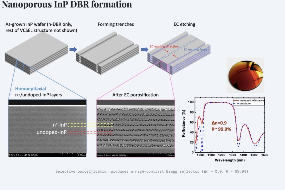
Figure 1. Engineers at imec have highlighted the potential of InP chiplets on a silicon interposer for millimetre-wave applications by demonstrating the low losses of this particular system.
When it comes to RF devices, it is even harder to determine what material to select. In part, that’s because one must consider more figures of merit, and determine their prioritisation on a case-by-case basis. Practical considerations are also challenging, with decisions needing to reflect how difficult it is to miniaturise a particular device and improve its high-frequency performance. So, given all these complications, it is helpful to know the state-of-the-art capabilities of RF transistors produced with a wide range of material systems.
An opportunity to get exactly that insight was given to delegates attending the most recent International Electron Devices Meeting (IEDM), held in San Francisco between 7th and 11th December. At that conference, and in the on-demand talks that followed, attendees could hear presentations on record-breaking RF devices made from a wide variety of material systems, including InP, GaN, AlScN, Ga2O3 and diamond.

Figure 2. (a) Intel has used 300 mm trap-rich SOI as a foundation for producing GaN MOSHEMTs on 300 mm silicon wafers. The thin silicon (111) layer serves as a crystalline template for GaN epigrowth. Beneath this is an underlying insulating buried oxide (BOX), and below that a trap-rich polysilicon layer that eliminates stray charges at the interface to the BOX, as well as a high-resistivity silicon substrate.
Marrying InP and silicon CMOS
Amongst the many materials that are suitable for producing RF transistors, InP offers a strong case as the leading option. By delivering an impressive performance, in terms of both gain and power efficiency, devices based on this III-V are compelling candidates for a number of millimetre-wave and sub-terahertz applications.
However, there is literally a high price to pay for the great performance of InP transistors. Their manufacture is costly, due to use of electron-beam lithography processes, and production on substrates that are at most 100 mm in diameter.
One application for InP transistors is phased arrays for radar systems. When these systems operate above 100 GHz, the antenna array pitch, which is governed by the operating wavelength, is of the order of 1 mm. This length scale necessitates the dense integration of InP power amplifiers and silicon CMOS beamformers.
An attractive approach to realising this integration, pioneered by the European microelectronics centre imec, is to position InP chiplets providing power amplification at precise positions on a fine-pitch carrier. The capabilities of this approach, using an RF silicon interposer platform developed in house, were highlighted at IEDM by imec’s Siddartha Sinha.

Figure 3. On 300 mm trap-rich SOI substrates, Intel has fabricated four
variants of the enhancement-mode high-k dielectric MOSHEMT. As well as
the standard form of MOSHEMT, there are those with a source field plate,
a gate field plate, and multi field plates.
There is a significant financial benefit that comes from combining InP and silicon CMOS in this way. “If you are able to restrict the III-V content in your design to less than 20 percent of your area, there is a drastic reduction in cost,” remarked Sinha, who added that these savings can be as large as a factor of five to ten. “We use InP only where it is needed, for RF power amplification, and everything else is built using standard CMOS technology.”
Sinha pointed out that there are four significant packaging challenges to overcome when producing platforms operating above 100 GHz: realising sufficiently dense integration; dealing with the fall in transistor performance that comes from scaling, overcome by introducing more stages or new materials; addressing high interconnect losses; and managing the increase in thermal density.
“At imec we have developed a unique interposer-based solution that addresses these four issues,” argued Sinha. He explained that he and his co-workers are able to realise dense integration with a 1 mm pitch for the arrays by using redistribution layers and a via pitch of 30 µm, and they tackle the decline in device performance with miniaturisation with a CMOS beamformer and InP power amplifiers. To reduce interconnect loss, imec’s engineers use smooth films of copper and low-loss polymers, and for thermal management they benefit from the use of silicon that has a much higher thermal conductivity than glass interposers.
To assess the capability of their technology, Sinha and co-workers have produced RF interposer stacks featuring: spin-coated layers on RF-friendly polymers, thick layers of copper that reduce low-frequency and DC losses, and interconnects that can operate up to 200 GHz (see Figure 1).

Figure 4. Using a strain-balanced design, engineers at Cornell have
broken the record for the frequency performance of AlScN/GaN HEMTs.
Transmission measurements on these interposers reveal line losses of 0.3 dB mm-1 and 0.23 dB mm-1 at 140 GHz for structures with polymer thicknesses of 15 µm and 22 µm, respectively. Broadband performance is realised, spanning 20 GHz to 170 GHz.
“These numbers are comparable to what you have in PCB or glass interposers, but with much higher integration densities – that is, much thinner substrate sizes,” remarked Sinha.
Additional investigations have considered the combination of the interposer and InP transistors.
To assess this, the team from imec flip-chip bonded a Teledyne 250 nm InP stack to its interposer with an in-plane alignment accuracy of 3 µm.
Passive measurements of losses with this flip-chip architecture determined values of 0.9 dB mm-1 and 0.3 dB mm-1 at 140 GHz for the InP backend microstrip and interposer microstrip, and an insertion loss of around 0.1 dB for one flip-chip transition over 20 GHz to 170 GHz.
“The interposer microstrip is about three times better than what you could get in an indium phosphide die back-end,” said Sinha, who added, “keep in mind that CMOS back-ends are even more lossy than this, because they are not millimetre-wave optimised.”
The engineers from imec have also investigated the active performance of the InP power amplifier on the interposer, recording a peak small-signal gain of 16.3 dB and a 3 dB bandwidth spanning 116 GHz to 148 GHz. “These are state-of-the-art numbers, compared to even standalone PAs,” claimed Sinha.

Figure 5. A collaboration from China has improved the performance of β-Ga2O3 MOSFETs by transferring chiplets of β-Ga2O3 to diamond using transfer printing.
GaN on 300 mm silicon
Another material with a proven pedigree for providing RF amplification is GaN.
One of the leading developers of this technology is Intel. Back in 2019 this chipmaker unveiled the industry’s first 300 mm GaN-on-silicon process for scaled enhancement-mode high-κ gate dielectric GaN MOSHEMTs for power delivery and RF electronics, and at IEDM 2024 it revealed that it had extended this technology with the introduction of a low-loss, high-resistivity engineered substrate. On this new platform, produced by Shin-Etsu Handotai and featuring a ‘trap-rich’ silicon-on-insulator architecture (see Figure 2 for details), Intel’s engineers have produced GaN MOSHEMTs with a 30 nm channel length that deliver a superior level of performance to those produced on a conventional silicon substrate.

Figure 6. The β-Ga2O3 MOSFETs formed on diamond using transfer printing feature an implanted channel and a T-shaped gate.
Spokesman for the team from Intel, Han Wui Then, told delegates at IEDM that engineered substates are important for the future of GaN. He explained that turning to a trap-tich poly-silicon layer ensures the elimination of stray charges at the interfaces to the buried oxide and to the high-resistivity silicon substrate. “This enables lower RF losses and better signal linearity; decoupling of the crystalline silicon (111) template from the silicon substrate; and acts as a clear separating or isolating layer that enables backside processing to realise advanced integration schemes that are chiplet-based, for example,” remarked Then.

Figure 7. β-Ga2O3 MOSFETs that feature a diamond foundation and are produced using transfer printing are setting new benchmarks for fT and fMAX for MOSFETs made with this ultra-wide bandgap oxide.
Measurements by the team show that switching from a high-resistivity substrate to the engineered one made by Shin-Etsu Handotai for growth of a GaN epilayer leads to a four-fold increase in effective electrical resistivity, along with superior linearity – there is 10 dB suppression of the second harmonic.
Using the novel trap-rich substrate, engineers from Intel have produced four variants of the enhancement-mode GaN MOSHEMT with a high-k dielectric at the company’s advanced CMOS fab in Oregon. As well as fabricating a standard form of MOSHEMT, they have produced another with a source field plate, a third with a gate field plate, and also a variant with a multi-gate architecture. All forms were fabricated using a 300 mm gate-last integrated process flow involving the epitaxy of GaN layers by MOCVD, the deposition of a high-κ dielectric, epitaxial re-growth of source and drain contacts, and the addition of a copper backend interconnect.

Figure 8. A partnership between engineers in Japan and the US has produced diamond MOSFETs with a Al2O3 high-k dielectric that operate at record-breaking frequencies.
Measurements on variants of the standard form of the GaN MOSHEMT with channel lengths of 30 nm, 90 nm, and 180 nm, show that these devices deliver enhancement-mode operation, have drive currents as high as 1 mA µm-1, and have an on-off ratio that exceeds 1010. These devices are said to have a good figure-of-merit for the RF switch – the product of the on-resistance and off-capacitance is 80 fs for a 30 nm channel length – and a good drain breakdown voltage, with a healthy breakdown slope of 1.3 MV cm-1.
The variant with the source-field plate is capable of drive currents exceeding 1 mA mm-1 and can handle drain voltage swings as high as 12 V. The cut-off frequency (fT) and maximum oscillation frequency (fMAX) are 190 GHz and 532 GHz, respectively. Note that the product of fT and fMAX is similar to that for Intel’s GaN-on-silicon MOSHEMTs on high-resistivity silicon.
For the gate-field MOSHEMT, current-voltage plots are similar to those of the source-field variant.
MOSHEMTs with two gates, separated by 150 nm, are less susceptible to short-channel effects, while maintaining a high drive current – it can be as high as 1.2 mA µm-1.

Figure 9. At IEDM 2024 a partnership between engineers in Japan and the US unveiled the world’s first diamond MMIC.
Improving the RF switch
The two primary choices of substrate for a GaN HEMT are SiC and silicon. GaN-on-SiC HEMTs offer a higher power-handling capability, but those with a silicon foundation are catching up, and offer the advantages of greater flexibility and superior economies of scale.
In this context, the downsides of the silicon substrate include degradation to devices and active components. A key circuit element that’s highly sensitive to the substrate is the RF switch, which must combine high linearity with a low insertion loss. To mitigate problematic substrate-induced surface losses, GaN-on-silicon devices tend to be produced using high-resistivity silicon substrates. However, while much effort has been devoted to studying the effects of GaN-on-silicon stacks on transmission-line RF loss and non-linearity, there have been very few investigations on active devices and RF switch circuits.
Helping to address this lack of knowledge is work at CEA-Leti involving the characterisation of GaN HEMT switches integrated on 200 mm high-resistivity silicon. This investigation, detailed at IEDM 2024 by Luca Lucci, is claimed to show that the GaN-on-silicon HEMT is approaching that of RFSOI, in terms of the metric that’s the product of on-resistance and off-capacitance, while offering linearity and power-handling capability previously only possible with GaN-on-SiC.
For this work, researchers at CEA-Leti have employed their own GaN-on-silicon process technology that involves processing epiwafers that feature an AlN nucleation layer, a GaN buffer layer, a 150 nm-thick GaN channel, a 700 nm-thick AlN spacer, a 20 nm-thick AlGaN barrier and a 7 nm-thick SiN cap, added in situ. HEMTs are produced from the epiwafers by using argon implants to realise isolation, prior to the addition of ohmic source and drain contacts annealed at just 590 °C. A T-shaped Schottky gate is then defined, before the addition of interconnects that are fully CMOS compatible.
Lucci presented measurements for losses from 0 GHz to 40 GHz for two different wafers. The more recent devices, associated with lower processing temperatures, had losses below 0.15 dB mm-1. “Our long-term target is to succeed in keeping these 30 gigahertz losses below 0.1 dB per millimetre, as is already feasible in gallium nitride on silicon carbide technologies,” remarked Lucci.
Small-signal measurements show that by trimming the size of the access region, the engineers at CEA-Leti are able to decrease the on-resistance while having just a very small impact in the off-capacitance. It’s also possible to reduce the off-capacitance while having a minimal impact on the on-resistance by reducing the width of the ohmic regions.
Showing a benchmarking plot of off-capacitance and on-resistance, Lucci remarked: “Our experimental points represent all the best of on-resistance, off-capacitance extracted so far from GaN-on-silicon technology, apart from data which has been published by Intel with a much, much shorter channel length of 40 nanometres.”
Lucci and co-workers have also carried out large-signal characterisation, determining that this technology can handle 36 dBm in a shunt configuration.
A benchmarking of all results led Lucci to conclude that his team’s technology still falls short of RFSOI, when judged on the product of on-resistance and off-capacitance. “But if we also put power handling in the picture – so the maximum power that the device can handle without requiring stacking in the design – that makes the GaN solution very attractive.” While GaN-on-SiC accommodates even higher powers, it requires gate voltages that are higher than preferable in many applications, according to Lucci.
Strain-balanced AlScN
For those believing that the AlGaN/GaN HEMT is starting to encroach its limits, switching the AlGaN barrier with another material has much appeal. Options include tensile-strained AlN, the lattice-matched ternary AlInN, and AlScN, which has a wider bandgap. The latter is a compelling candidate: it’s not impeded by a 6 nm strained-related thickness limitation that impairs AlN, or restricted to a two-dimensional electron gas density of no more than 2 x 1013 cm-2, a limitation that holds back AlInN.
Development of the AlScN/GaN HEMT is in its infancy. Early reports provided a value for fMAX of no more than 156 GHz, but far higher values are possible, according to recent research from Cornell University that pairs compressively strained AlScN with tensile strained AlN.
Unveiling this breakthrough at IEDM 2024, Cornell’s Thai-Son Nguyen explained that these record-breaking HEMTs were produced by loading high-resistivity 4H-SiC substrates into a MBE reactor and depositing a 100 nm-thick AlN nucleation layer, followed by a unintentionally doped 600 nm-thick layer of GaN, a 1.5 nm-thick layer of AlN, a 5 nm-thick layer of Al0.87Sc0.13N, and a 2 nm-thick GaN cap, added to prevent oxidation of the aluminium-containing epilayers.
According to Hall effect measurements on this epistructure, the sheet charge is 2.46 x 1013 cm-2, the mobility 755 cm2 V-1 s-1, and the sheet resistance 337 Ω/sq.
To produce HEMTs from epiwafers, Nguyen and co-workers employed hard mask patterning and etching, followed by the addition of MBE-regrown source and drain n+ contacts. Processing continued with device isolation, ohmic metallisation of source and drain contacts, and the use of electron-beam lithography to construct T-shaped gates with a length of 40 nm.
Electrical measurements determined a contact resistance for the ohmic contacts of 0.09 Ω mm. “This is the lowest contact resistance reported for AlScN/GaN HEMTs, and is in line with some of the best contact resistances for GaN HEMTs in general,” remarked Nguyen.
He and his colleagues have compared the performance of AlScN/GaN HEMTs with gate lengths of 800 nm, 120 nm and 40 nm. They found that the maximum drain current increases with scaling, to exceed 2.5 A mm-1, and on-resistance can be as low as 0.83 Ω mm.
Small-signal RF results on the HEMT with the shortest gate length determined values for fT and fMAX of 173 GHz and 321 GHz, respectively. “These are the highest fT and fMAX reported for AlScN HEMTs,” remarked Nguyen (see Figure 4 for values of fT and fMAX at various gate lengths). He predicts that even higher values are possible with more extreme scaling, such as a 20 nm gate length.
Combining Ga2O3 with diamond
Over the last few years interest in Ga2O3 power devices has rocketed, driven by this oxide’s high breakdown field, as well as the promise of low-cost, high-quality native substrates. Note, though, that Ga2O3 also has much promise in the RF domain – it is three times better than GaN, according to a Johnson figure of merit that characterises power-frequency capability.
The Achilles heel of Ga2O3 is its incredibly poor heat dissipation. This can be addressed by pairing this oxide with materials that are far better in this regard, such as diamond, well-known for its exceptional thermal conductivity. However, combining Ga2O3 and diamond is far from easy. Severe lattice mismatch between them hinders direct epitaxial growth, and direct wafer bonding is problematic, due to dangling bonds created during the activation process.
Offering a far more promising alternative, unveiled at IEDM 2024 by a collaboration from China, is a transfer printing process that forms arrays of β-Ga2O3 thin films and MOSFETs on diamond. Triumphs by this team from Shanghai Institute of Microsystems and Information Technology, Nanjing Electronics Devices Institute, the National Key Laboratory of Solid-Sate Microwave Devices and Circuits, and Harbin Institute of Technology, include record-breaking frequencies for their devices.
To produce their arrays, this partnership begins by using its novel ion-cutting technology to fabricate a 2-inch β-Ga2O3/SiO2/silicon wafer. After using inductively coupled plasma to etch a square pattern into the β-Ga2O3 layer with dimensions of 200 µm by 200 µm, these engineers remove the exposed SiO2 layer by etching in HF acid for 4 hours to ensure a direct contact between β-Ga2O3 and the silicon substrate. Coating the whole wafer with polyvinyl alcohol follows, before transfer printing exploits the weak van der Waals interaction between β-Ga2O3 and silicon, and unites the β-Ga2O3 chiplets with a 1-inch diamond substrate. Deionised water then dissolves the polyvinyl alcohol, prior to annealing at 900 °C for 30 minutes, to strengthen the bond between β-Ga2O3 and diamond (see Figure 6 for an illustration of the process).
Spokesman for the team, Tiancheng Zhao from the Shanghai Institute of Microsystems and Information Technology, told delegates at IEDM that the team confirmed the quality of the transferred film using X-ray diffraction and atomic force microscopy. There is an X-ray diffraction peak around just 78 asrcec wide, highlighting the lack of stress in the film.
Zhao explained that HF acid etching damages the surface of the films, with a root-mean-square value for roughness, according to atomic force microscopy, of 0.59 nm. However, planarization via an inductively coupled plasma improves surface quality, reducing the root-mean-square roughness to just 0.36 nm.
Further evidence for the high-quality of the transfer process comes from cross-sectional transmission electron microscopy. This technique reveals a well-organised lattice arrangement for the β-Ga2O3 thin film, and a well-defined, sharp heterointerface – the amorphous layer between β-Ga2O3 and diamond is less than 2 nm-thick. “This is beneficial for the transport of interface phonons,” remarked Zhao.
He and his co-workers have benchmarked the thermal boundary resistance of their process for uniting β-Ga2O3 and diamond. The value they have obtained, 21.7 m2 K-1 GW-1, is significantly better than that for a number of alternatives, including mechanical exfoliation.
To produce devices from the array of β-Ga2O3 films on diamond, Zhao and colleagues thin down the β-Ga2O3 and smooth its surface, before isolating the mesa, using ion implantation to form a channel, and adding source and drain ohmic contacts, followed by a 15 nm-thick film of Al2O3 gate dielectric and a T-shaped gate (see Figure 6).
Electrical measurement on the β-Ga2O3 MOSFETs have revealed a maximum drain current of 810 mA mm-1, a value more than three times that of a bulk variant. Values for fT and fMAX are 34 GHz and 61 GHz, respectively, with the latter breaking new ground for β-Ga2O3 MOSFETs (see Figure 7). This success is attributed to the combination of an undamaged β-Ga2O3 film, a high-quality interface, and the diamond substrate’s high thermal conductivity and low parasitic effects.
Diamond devices
The exceptional thermal conductivity of diamond, alongside its high breakdown field and high thermal conductivity, make this ultra-wide bandgap semiconductor a very promising candidate for producing high-frequency devices. Conventional bulk doping is far from ideal, due to the high activation energy, but it is possible to form a two-dimensional hole gas near the surface of this allotrope of carbon.
For several decades, researchers have been developing diamonds transistors. These efforts have identified that the performance of the diamond RF MOSFET falls far short of the limitations of this material, and that device performance hinges on transconductance, which can be improved with high-k dielectrics. Recent work has identified the benefits of an Al2O3 gate, and variants with a higher permittivity, such as HfO2, have much promise.
At IDEM 2024 a partnership between researchers in China and the US revealed that diamond devices with a HfO2 dielectric can fulfil their potential. This team from Nanjing Electronics Devices Institute, the National Key Laboratory of Solid-Sate Microwave Devices and Circuits, Nanjing University and Virginia Tech, reported that diamond MOSFETs with a HfO2 dielectric deliver record-breaking values for fT and fMAX. The team have used them to produce the first ever diamond MMIC.
Record-breaking devices were formed by depositing a 50 nm-thick gold film on a hydrogen-terminated diamond surface by electron-beam evaporation, before removing the gold outside the active regions by chemical treatment, and using oxygen plasma to provide electrical isolation. Following electron-beam lithography, channels were opened by wet etching gold, before using atomic layer deposition to add a 10 nm-thick film of HfO2, employed as both the gate insulator and passivation dielectric. To complete the MOSFET, the team added a T-shaped gate (see Figure 8 for an overview of the process).
Electrical measurements revealed that the two-dimensional hole gas has a density of 8.9 x 1012 cm-2 at room temperature, rising to 9.2 x 1012 cm-2 at 200 °C. Mobility decreases by just 34.5 percent over this temperature range. In comparison, for a GaN HEMT, the mobility of its two-dimensional electron gas falls by 70 percent between room temperature and 200 °C.
Diamond MOSFETs with a gate length of 80 nm produce a peak drain current of 1.05 A mm-1 and a transconductance of 251 mS mm-1. Measurements of small-signal characteristics determined values for fT and fMAX of 90 GHz and 164 GHz, respectively, and large-signal characteristics at 20 GHz revealed an output power density of 230 mW mm-1.
The engineers have produced a diamond MMIC for operation in the X-band that has dimensions of 1.7 mm by 0.8 mm. Small-signal gain peaks at 6.25 dB at 7 GHz. At 10 GHz, this MMIC produces a small-signal gain of 6.25 dB, and an output power of 117 mW (see Figure 9).
This work, and that of the other team’s presenting at IEDM, highlights improvements in RF performance realised by devices made from many material systems. All offer promise, but will they kick on to commercial success over the coming decades? Only time will tell.