Germanium’s great versatility
As well as providing a great foundation for multi-junction solar cells and VCSELs, germanium substrates can provide a unifying force between the compounds and the silicon industry.
BY BENDIX DE MEULEMEESTER FROM UMICORE
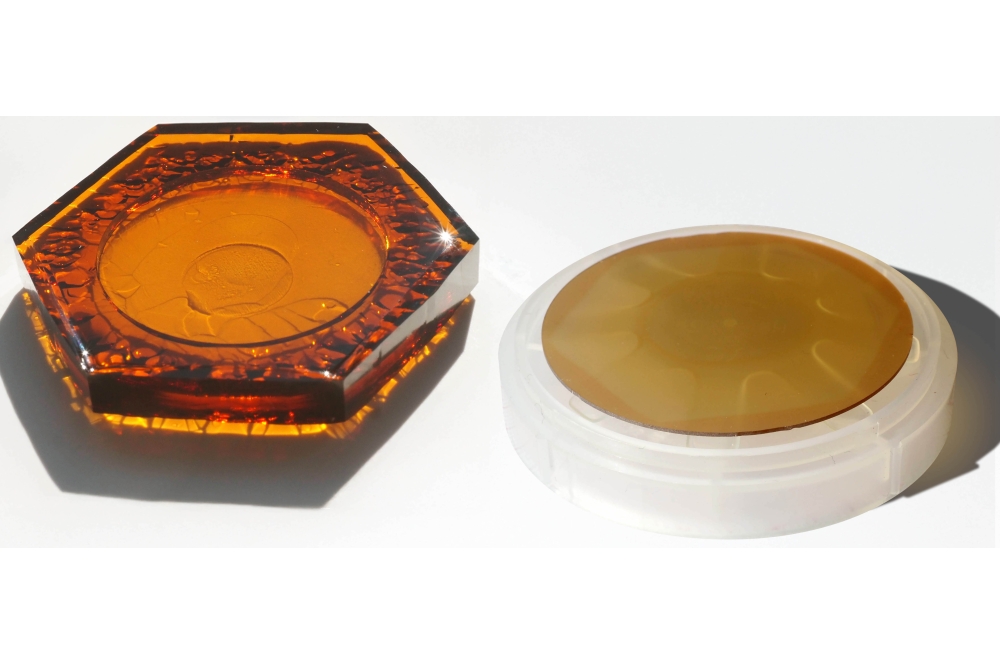
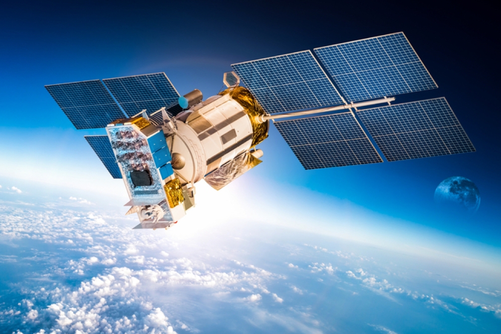
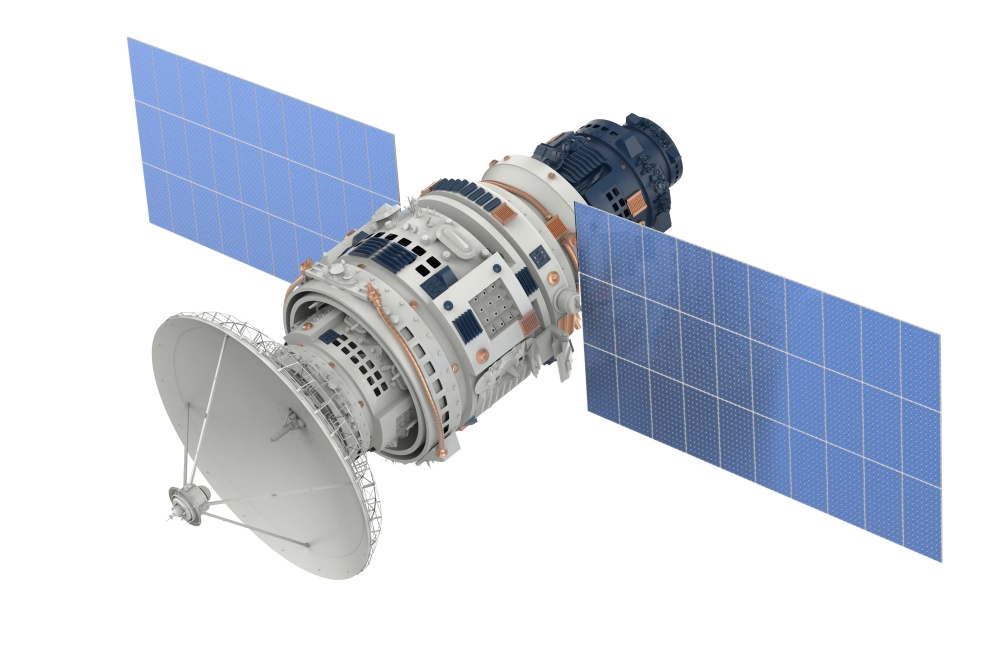
What is the germanium substrate used for? If you are a veteran of this industry, you’ll surely have an answer to this, as you’ll know that it is widely used as the bedrock for producing multi-junction solar cells, which now power numerous satellites orbiting our planet. That’s the market that sparked the launch of the commercial germanium substrate in the 1990s, and accounted for all of its use for the first 20 years or so. But during the last decade, this platform has started serving other applications, a direction of travel that is sure to continue. You might be aware of some of these new uses – but there’s a good chance that others will come as a surprise.
On the back of the success of highly efficient multi-junction cells in space, many companies tried to diversify this technology to the terrestrial solar market. Interest in this rocketed during the beginning of this century, before pioneers were forced to abandon their plans, thwarted by plummeting prices for silicon panels and a global credit crunch that chocked investment.
Now, though, there is hope of a rival, with a modified form of concentrated photovoltaics, which combine the generation of electricity from the sun’s rays with the storage of thermal energy. The latter allows the opportunity to power the grid precisely when it is needed. For this new form of green-energy generation, solar cells must be as thin as possible to ensure efficient cooling and recovery of heat. Addressing this requirement is a cost-effective germanium wafer re-use technology, currently under development and testing, that could provide a compelling alternative to the substrate thinning approach performed by a grinding process.
Optoelectronic opportunities
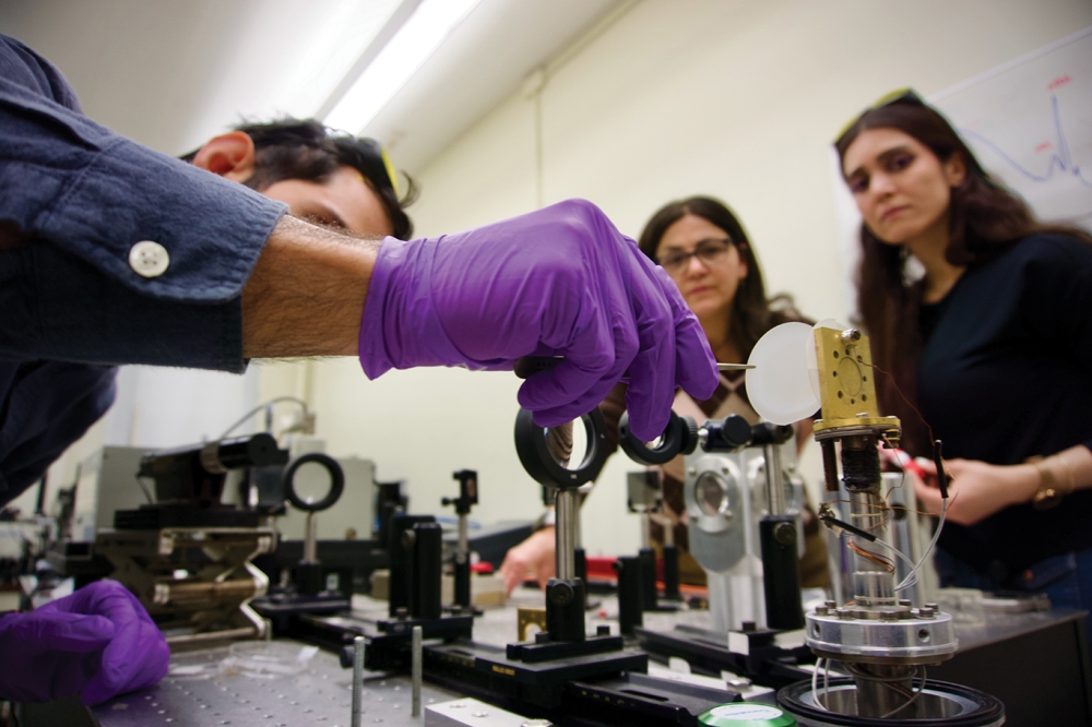
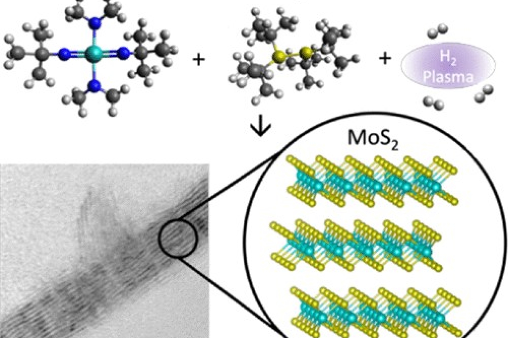
Over the last few years, the usage of germanium substrates has started to branch out into other optoelectronic applications. You may have come across the development of GaAs-based VCSELs on this foundation. Interest in this particular substrate stems from its superior material properties, compared with GaAs, for epitaxial growth of compound semiconductors. Key merits of germanium are a lattice constant between that of GaAs and AlAs, and a matching thermal expansion coefficient. These attributes make germanium an ideal substrate for the epi-growth of photonic devices incorporating distributed Bragg reflectors based on the pairing of GaAs and AlAs.
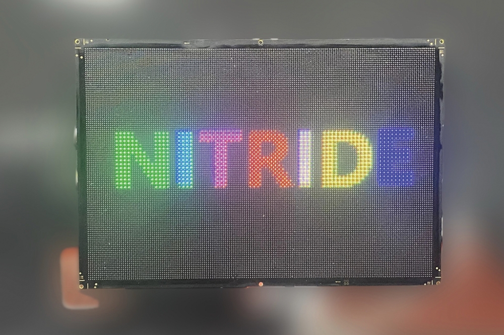
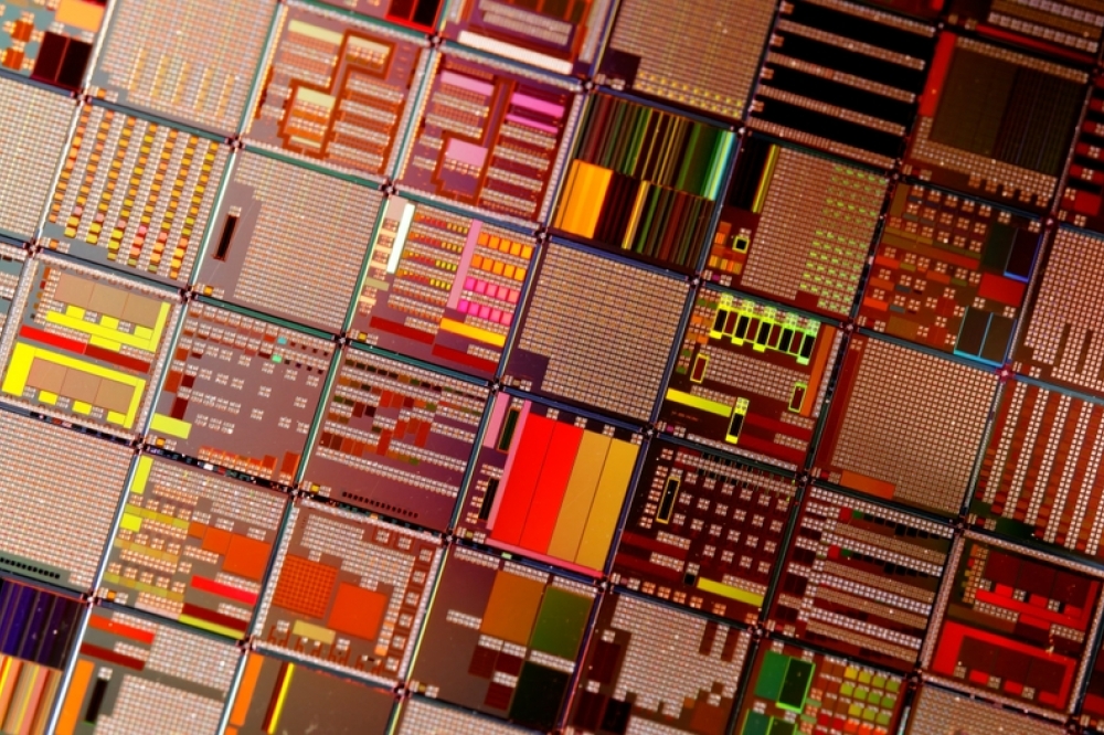
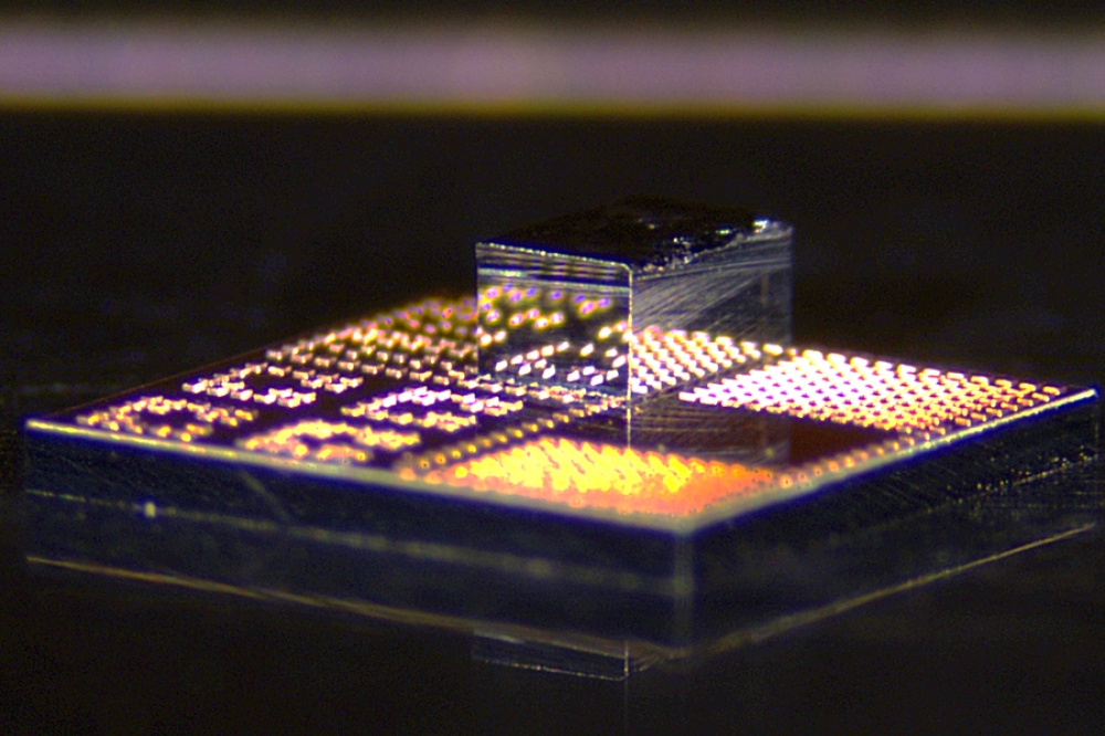
The VCSEL is by no means the only optoelectronic device that can benefit from germanium. This substrate could offer great value in next-generation, high-volume photonic applications, such as microLEDs, still a promising source for displays, despite Apple’s headline-grabbing decision to move away from working with ams Osram. High volumes will be aided by the size of this foundation, available in the form of dislocation-free wafers with diameters of 200 mm and even 300 mm. As well allowing for more devices to be fabricated per wafer, significantly improving throughput and reducing cost per device, these large wafers have the advantage of enabling processing in state-of-the-art silicon foundries. Utilising existing silicon manufacturing infrastructure is a big win, slashing costs and streamlining production processes.
Note that after the growth of microLEDs on germanium, substrate removal is required to enable integration with the backplane. The good news is that substrate removal technology is advancing, due to efforts in concentrated photovoltaics.
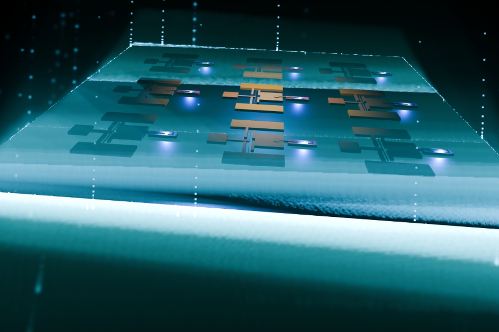
It is also possible to integrate III-V photonics on germanium substrates, opening new avenues for device architecture and functionality. These new directions can involve the monolithic integration of photonic and electronic components, essential for developing more compact and efficient high-performance optoelectronic systems. Integration is particularly beneficial in space-limited high-volume consumer applications, such as time-of-flight-based depth sensors.
What’s more, engineers can draw on the low-bandgap of germanium to support their development of advanced photonic devices for data communication in the short-wave infrared. And there are opportunities to exploit next-generation complementary FETs, with improved performance characteristics.
A logical extension
Even more exciting is the radical move of integrating compound semiconductors with existing silicon logic platforms. This holds profound implications for the advancement of photonics and electronics, promising enhancements in performance, efficiency, and scalability that were previously challenging to achieve.
With so many opportunities for the germanium substrate, are there concerns over material supply? No – and that will remain, given that germanium recycling is easy. The substrate can be removed by grinding or selective etching, and germanium can be 100 percent recycled for re-use, limiting reliance on primary raw materials.
Thanks to such a promising future, which is not held back by supply issues, there’s a very bright future ahead for germanium.