
MIT reveals 3D mmWave GaN on CMOS tech
Researchers from MIT and elsewhere have developed a new fabrication process that integrates high-performance GaN transistors onto silicon CMOS chips in a way that is low-cost, scalable, and compatible with existing semiconductor foundries.
The research ' 3D-Millimeter Wave Integrated Circuit (3D-mmWIC): A Gold-Free 3D-Integration Platform for Scaled RF GaN-on-Si Dielets with Intel 16 Si CMOS' was presented at the recent IEEE Radio Frequency Integrated Circuits Symposium (15 - 17th June) in San Fanscisco.
The method involves building many tiny transistors on the surface of a GaN chip, cutting out each individual transistor, and then bonding just the necessary number of transistors onto a silicon chip using a low-temperature process that preserves the functionality of both materials.
The team says that the cost remains minimal since only a tiny amount of GaN material is added to the chip, but the resulting device can receive a significant performance boost from compact, high-speed transistors. In addition, by separating the GaN circuit into discrete transistors that can be spread over the silicon chip, the new technology is able to reduce the temperature of the overall system.
The researchers used this process to fabricate a power amplifier that achieves higher signal strength and efficiencies than devices with silicon transistors. In a smartphone, this could improve call quality, boost wireless bandwidth, enhance connectivity, and extend battery life.
“We’ve combined the best of what exists in silicon with the best possible GaN electronics. These hybrid chips can revolutionise many commercial markets,” says Pradyot Yadav, an MIT graduate student and lead author of a paper on this method.
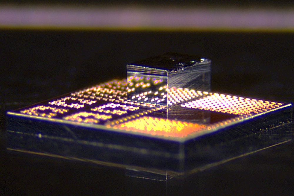
The new chips are the result of a multistep process. First, a tightly packed collection of transistors is fabricated across the entire surface of a GaN wafer. Using very fine laser technology, they cut each one down to just the size of the transistor, which is 240 by 410 microns, forming what they call a dielet.
Each transistor is built with tiny copper pillars on top, to bond directly to the copper pillars on the surface of a standard silicon CMOS chip. Copper to copper bonding can be done at temperatures below 400 degC, which is low enough to avoid damaging either material.
Current GaN integration techniques require bonds that use gold, an expensive material that needs much higher temperatures and stronger bonding forces than copper. Since gold can contaminate the tools used in most semiconductor foundries, it typically requires specialised facilities.
“We wanted a process that was low-cost, low-temperature, and low-force, and copper wins on all of those related to gold. At the same time, it has better conductivity,” Yadav says.
To enable the integration process, they created a specialised new tool that can carefully integrate the extremely tiny GaN transistor with the silicon chips. The tool uses a vacuum to hold the dielet as it moves on top of a silicon chip, zeroing in on the copper bonding interface with nanometer precision.
Advanced microscopy is used to monitor the interface, and then when the dielet is in the right position, heat and pressure is applied to bond the GaN transistor to the chip.
“For each step in the process, I had to find a new collaborator who knew how to do the technique that I needed, learn from them, and then integrate that into my platform. It was two years of constant learning,” Yadav says.


