
Shrinking the size of LiFi through heterogeneous integration
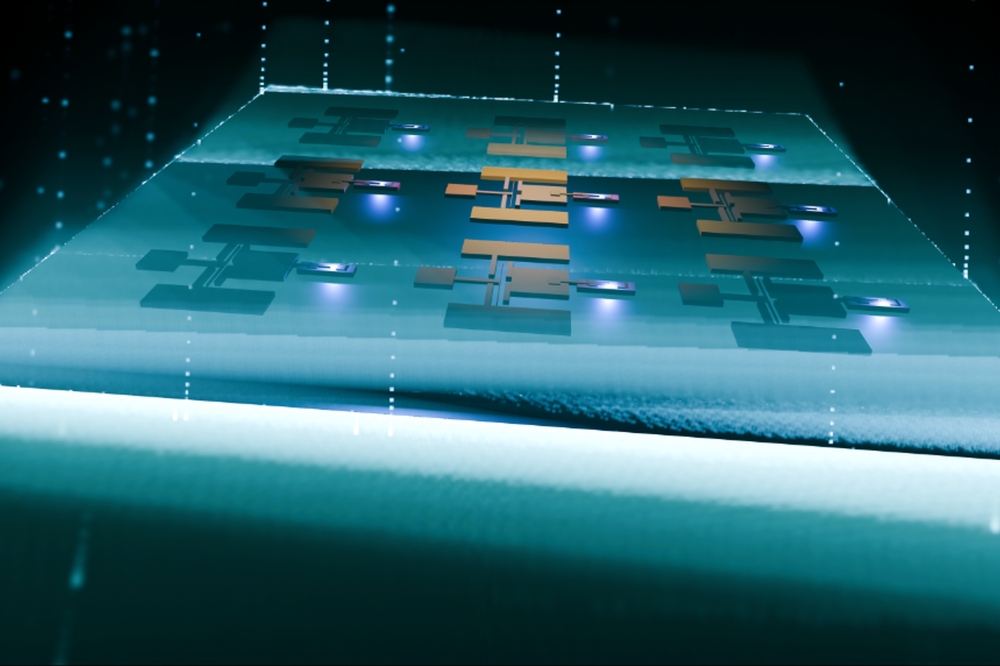
Combining microLEDs and GaN HEMTs via transfer printing creates chip-scale systems that are opening new possibilities for visible light communication.
BY MUHAMMET GENC, ZHI LI, BRENDAN ROYCROFT AND BRIAN CORBETT FROM TYNDALL NATIONAL INSTITUTE AND SHEIKH IFATUR RAHMAN AND SIDDHARTH RAJAN FROM OHIO STATE UNIVERSITY
Within the field of wireless communication, visible light communication (VLC) has emerged as a transformative technology that’s gaining increasing attention over traditional Radio Frequency (RF)-based communication methods.
At the heart of many of these VLC systems are LEDs, transmitting data at high speeds. These sources provide a promising solution to the challenges posed by crowded RF spectrums that are straining to satisfy the growing demand for higher data rates.
Migrating to the unlicensed visible light spectrum, which spans 400 THz to 800 THz, accesses a vast bandwidth, enabling VLC systems to support faster communication speeds with minimal interference, even in environments where RF signals are congested or impractical.

Figure 1. MicroLED release, transfer, and integration process. (a)
Undercutting of microLEDs from the silicon substrate via selective
etching using a tetramethylammonium hydroxide (TMAH) solution. (b) Image
showing the microLEDs still securely attached to the SiN anchors
following the etching process. (c) Transfer of the microLEDs onto a
GaN-based HEMT structure on a SiC substrate. (d) High-magnification view
of the final transfer of the microLEDs onto the GaN-based HEMT
structure on the SiC substrate.
VLC is poised make a valuable contribution in many emerging applications, including smart cities, autonomous vehicles, the Internet of Things (IoT), and Artificial Intelligence (AI)-powered data centres. In all these examples, there is increasing need for high-speed, reliable communication systems that handle vast amounts of data. VLC offers a strong solution for addressing these demanding requirements, particularly in high-density indoor environments, such as office spaces, airports, conference halls, shopping malls and smart homes. For IoT applications, the appeal of VLC may be particularly strong compared with RF-based communication when deployed in environments where interference, limited bandwidth, or regulatory constraints make RF impractical.
In the autonomous vehicle, VLC could be a game changer, rather than just an attractive alternative. That’s because VLC might facilitate real-time communication between vehicles, pedestrians, and infrastructure, and enable faster, more reliable decision-making. This could significantly enhance the safety and efficiency of transportation systems.
Meanwhile, in AI data centres VLC has the potential to revolutionise communication in chip-to-chip optical interconnects by enabling ultra-fast data transfer between components – this is essential for emerging computing technologies.
Despite much interest in the successful commercialisation of VLC systems, roll-out is held back by a number of technical challenges. While the leading candidate for the light source is clear – it’s microLEDs made from GaN, which is renowned for its high efficiency, brightness, and ability to operate at high frequencies – it’s far from easy to integrate these emitters with high-speed electronics that’s capable of handling the modulation and control of these light sources.
Under the Tyndall National Institute/Ohio State University Catalyst Project, led by Muhammet Genc and Siddharth Rajan from the respective insitutions, we have teamed up to address key challenges in VLC technology. Our innovative approach, which involves integrating GaN-based microLEDs with GaN HEMTs on a single chip platform, aims to simplify VLC system design while significantly reducing size and improving energy efficiency. This work holds the potential to enable scalable, cost-effective, high-speed data transmission using visible light, laying a strong foundation for the next generation of optical communication systems.

Figure 2. Modulation of microLED by GaN HEMT during operation.
The integration challenge
In traditional VLC systems, external drivers provide the high current densities required for high-speed modulation of the microLEDs. However, these external components add size and complexity to the system, reducing overall efficiency and scalability. What’s more, the power consumption of these external drivers increases the overall energy demands of VLC systems, making them less suitable for small, portable consumer devices.
Our solution to this challenge lies in the integration of GaN microLEDs with GaN HEMTs, which are well-suited for high-speed modulation. HEMTs are capable of driving large currents with minimal resistance, and are known for their high electron mobility, making them ideal for controlling the operation of GaN microLEDs. Integrating these two components onto a single chip eliminates the need for external drivers, simplifying system architecture and reducing energy consumption. This approach has the potential to pave the way for compact, high-performance VLC systems that are more energy-efficient and scalable.
We integrate our GaN-based microLEDs and GaN HEMTs onto a single chip with a novel transfer printing technique. This ensures precise placement of microLEDs onto the GaN HEMT substrate without damaging delicate components. Our process begins by fabricating GaN microLEDs on a silicon substrate, and patterning and etching them into the desired shape – we choose dimensions of 20 µm x 10 µm. Following the preparation of our microLEDs, we release them from the silicon substrate via selective etching, with SiN tethers holding them in place during the release process (see Figure 1 (a) and (b)).
The microLEDs are then transferred to a flexible polydimethylsiloxane (PDMS) stamp, which ensures accurate alignment for transfer to the GaN HEMT wafer. Using this transfer printing process, we ensure precise placement of the microLEDs onto the HEMT substrate without the risk of damaging the components (see Figure 1 (c) and (d)). After transfer is complete, we thoroughly test the chips to assess their electrical and optical performance. Our process ensures successful integration of GaN microLEDs and GaN HEMTs, creating a single chip that combines the high-speed modulation capabilities of the HEMTs with the optical performance of the microLEDs. Ultimately, we are capable of producing a highly efficient VLC system.
We view our integration process as a significant step toward the miniaturisation of VLC systems, as it reduces the need for bulky external drivers and simplifies the overall design. The result is a compact, energy-efficient system that can be easily scaled for a wide range of applications previously discussed.

Figure 3. Electro-optical and frequency characteristics of
transfer-printed microLEDs integrated with GaN HEMTs on a single-chip
platform. (a) Light-current-voltage (L-I-V) characteristics of a 20 x 10 µm2 microLED. (b) Drain-source current (Ids) as a function of supply voltage (Vdd) for various gate voltages, with Ids
reaching zero at a gate voltage of -4 V. (c) EL intensity versus gate
voltage, indicating a decrease in EL intensity as the gate voltage
exceeds -4.2 V, confirming the “off” state. (d) Power versus frequency
(log scale) for different current levels (2 mA, 3 mA, and 4 mA) at a
gate voltage of -3.2 V, showing a 3 dB modulation bandwidth of 100 MHz,
demonstrating the dynamic frequency response of the integrated
microLED-GaN HEMT device.
Demonstrating success
After successfully integrating our GaN microLEDs and GaN HEMTs, we subjected the resulting system to rigorous testing to evaluate its performance (see Figure 2). Our efforts began by measuring the light-current-voltage characteristics of our microLEDs. These devices demonstrated a turn-on voltage of 2.6 V and a maximum optical power output of 0.24 mW at a current density of 250 A cm-2. Our results confirm that these emitters are capable of efficient light emission, even at high current densities (see Figure 3 (a)).
Next, we assessed the modulation capabilities of our integrated system. By adjusting the gate voltage of the GaN HEMT, to control current flowing through the microLED, we realised precise modulation of the light emission, a key requirement for high-speed VLC. Our system successfully modulated the light emission of the microLEDs, with the drain-source current of the GaN HEMT dropping to zero at a gate voltage of -4 V, indicating that the modulation process was functioning as expected (see Figure 3 (b) and (c)).
One of our most valuable tests has involved evaluating the modulation bandwidth of the system. This determined a 3 dB modulation bandwidth of 100 MHz, which, while not yet sufficient for next-generation VLC applications, represents a promising result for this first-generation integration of microLEDs and HEMTs. The 100 MHz bandwidth indicates that our system is capable of high-frequency operation, providing a solid foundation for future improvements in modulation speed and overall performance (see Figure 3 (d)).
Future implications
Our successful integration of GaN-based microLEDs and GaN HEMTs onto a single chip offers several key advantages for the future of VLC. First and foremost, it eliminates the need for external drivers, significantly reducing the size, complexity, and energy consumption of VLC systems. This makes VLC a more viable option for portable devices, such as smartphones, wearable technologies, and IoT gadgets, where space and energy efficiency are critical. Additionally, our VLC technology can directly benefit advanced applications in AI data centres, where fast and reliable optical interconnects are crucial for massive data processing.
Moving forward, we will focus on increasing the modulation bandwidth of our system, with the goal of reaching speeds in the gigahertz range and beyond. If we achieve such high modulation speeds, this will allow VLC systems to handle the demanding data rates of modern communication networks, making them viable alternatives to RF-based systems for a variety of applications, including chip-to-chip optical interconnects in high-performance computing environments and AI data centres.
Another area for future development is improving the scalability of the integration process. While the transfer printing technique that we have used in this study is highly effective for integrating GaN microLEDs with HEMTs, there are opportunities to enhance the scalability of this process and make it suitable for mass production of VLC systems.
It may also be possible to increase the performance and the efficiency of our VLC systems by introducing integration techniques that incorporate other electronic components, such as photodetectors.
Our triumph – the integration of GaN-based microLEDs with GaN HEMTs onto a single chip – marks a significant milestone in the development of compact, energy-efficient VLC systems. By eliminating the need for external drivers, we have simplified system design, trimmed power consumption, and opened-up new possibilities for high-speed, interference-free communication. While the modulation bandwidth of 100 MHz is an important first step, we know that further advances in modulation speed and system scalability are necessary to unleash the full potential of VLC in a range of emerging applications, including AI data centres, chip-to-chip optical interconnects, and other high-performance communication networks. As we continue to develop this technology, this will increase its potential for shaping the future of wireless communication in a wide range of industries.


