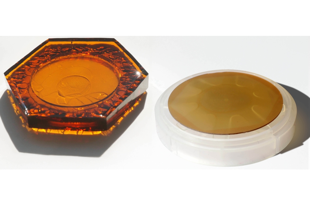
EU project to provide 4 inch AlN crystals
Three leading players in semiconductor research and development – the Leibniz Institute for Crystal Growth (IKZ), the PVA TePla AG, and the Siltronic – are combining their expertise in a pioneering project to scale up aluminium nitride (AlN) crystal growth.
The project focuses on the fabrication of 4-inch AlN substrates to enable applications in high-power electronics and ultraviolet photonics.
The project's focus on scaling AlN crystal diameters from 2 to 4 inches addresses a fundamental requirement for transitioning this key material from research-scale to industrial manufacturing environments.
The Leibniz Institute for Crystal Growth (IKZ) brings its long-standing expertise in growing AlN crystals to the project and has a proven 2-inch AlN crystal growth platform.
Siltronic. a producer of silicon wafers (using both Czochralski and Float Zone methods), contributes its experience in in the R&D of substrates for power electronics and in precision metrology.
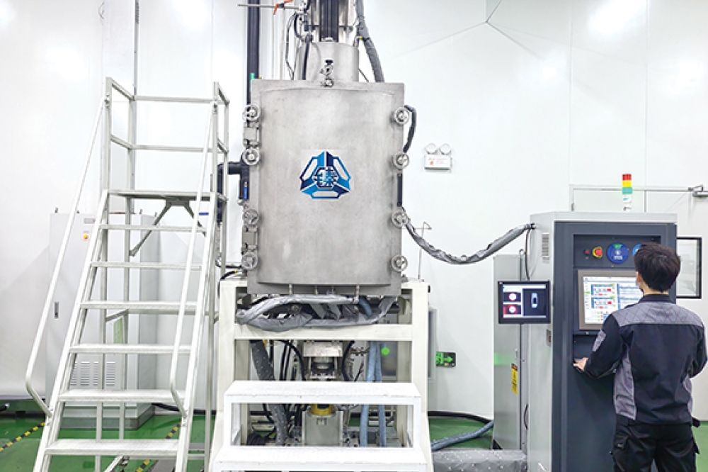
PVA TePla AG provides solutions in materials and metrology with decades of experience in manufacturing crystal growing systems. With its expertise in the Physical Vapour Transport (PVT) method, particularly in the SiC market, PVA TePla provides the equipment for growth process for bulk AlN crystals.
“The expansion from 2-inch to 4-inch is a crucial milestone in making AlN accessible for mass production”, the project partners explain. “Thanks to the synergies among the partners, we can overcome the technological barriers.”