CMOS: Not just for silicon

While CMOS may be synonymous with the manufacture of silicon ICs, it’s a versatile process can also be applied to the production of photonic and microwave circuits employing compound semiconductors.
BY JAMES PAN FROM NORTHROP GRUMMAN
Silicon ICs – invented in 1950s – are used in almost everything. Better known for their deployment in smartphones and computers, they are also integral to the operation of automobiles, washing machines, air conditioners, vacuum cleaners and so on. In all these cases, the ICs operate in total darkness, because silicon has an indirect bandgap. Due to this characteristic, silicon can absorb light, but it cannot emit it.
In our daily life, electrons and light are intertwined. We use electrons to generate light and other forms of electromagnetic radiation, such as microwaves. And while we might think of photons when we think about lasers and LEDs, they are electron devices – as are radar and lidar.
Now we need to start applying the principle of working with electrons and photons, which are intertwined, in ICs. Development is already underway, as compound semiconductors, such as GaAs, InP, and other III-V and II-VI compounds, are now used with silicon. Consider, for example, microwave photonic CMOS, which includes III-V or II-VI materials for lasers or millimetre-wave diodes, in the CMOS drain region, through a process called ‘selective epitaxy’.
Figure 1. Microwave photonic CMOS and image sensors. Positive feedback
loops convert light to light currents. Photon-accelerated microwave
generation produces modulated light wave and millimetre wave signals.
It’s possible that these ideas might strike you as a little odd. I’m sure you have heard of the acronym CMOS – its full name ‘complementary metal-oxide semiconductor’ – and you’ll know that it’s a process employed to make billions of silicon ICs. But it’s quite possible that this is the extent of your knowledge. And, to be fair to you, why should you know any more than this, given that many will believe that CMOS is not of any relevance to the compound semiconductor industry.
Well, I understand your position – but you are in danger of falling behind the times. Change is now afoot, thanks in part to our work at Northrop Grumman, a leader of lasers, millimetre-wave devices, and ASICs (Application Specific Integrated Circuits). We are developing a CMOS process for light-emitting structures and microwave circuits. It’s a revolutionary breakthrough that will enable the integration of both compound semiconductors and silicon for almost ‘all products’ in the $500 billion CMOS industry, which is growing rapidly.
Figure 2. Ultra-High-Speed Microwave Photonic Vertical NAND FLASH.
Our efforts are not the first to unite silicon and the compounds in ICs. Long gone are the days when silicon photonics is a new entity, having been pioneered by companies such as IBM and Intel, with products forming a small part of the IC industry. Today silicon photonics has already entered ULSI (Ultra Large-Scale Integration) markets, a point well-illustrated by the delivery of a webinar last August by Global Foundry’s Anthony Yu, who gave a presentation entitled Bringing Silicon Photonic Technology to the Forefront). Within this development there’s microwave photonic CMOS, involving modern processors that include hundreds of billions or trillions of CMOS transistors.
Based on such activities, a new trend is emerging – most, or even all of these many billions of CMOS transistors are no longer going to be fabricated only in silicon. Instead, they will incorporate GaAs, InP, or other compound semiconductors used in lasers and LEDs.
Behind this revolution is the move in modern societies to replace wireless tools with non-wireless tools, a migration observed in the uptake of smartphones, and changes to the connectivity of computers. In this particular case, the advantages of implementing compound semiconductors with silicon are wireless ULSI, and eliminating heating of the copper wires, and delays associated with their resistance and capacitance. There’s the promise of replacing billions of copper wires in ULSI with wireless photonic CMOS technologies.
Figure 3. Wireless ULSI with Photonic CMOS – significant reduction of RC delays and heat.
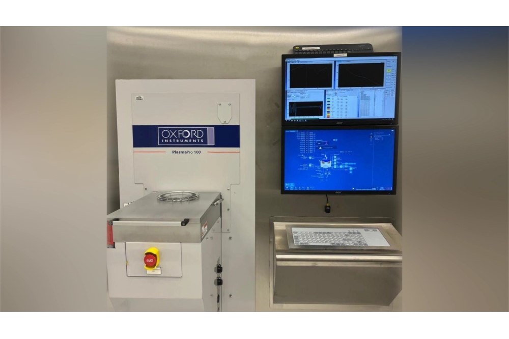
You may be wondering how III-Vs are introduced using a CMOS process. One illustrative example is the addition of GaAs in the CMOS silicon drain region, using either low-temperature selective CVD or selective epitaxy. For the former, the CVD tool includes an in-situ chamber in ultra-high vacuum, where native oxides on silicon are sputtered and etched, prior to sending the wafer to the CVD chamber for GaAs epitaxy. Note that all these processes proceed under high vacuum.
As GaAs is deposited right before the silicide process, in the BEOL (Back End of the Line), there are no contamination concerns, enabling the use of silicon lines (see Figure 1 for an illustration of the process integration of photonic CMOS).
Thanks to the introduction of III-Vs, the era of microwave photonic CMOS is within our grasp. For this technology, options for the optical source include GaAs LEDs, emitting in the 800 nm to 900 nm range, threshold-less tunnel lasers on silicon, and microwave-generating devices. Note that microwave photonic CMOS can outperform traditional laser diodes, due to improved thermal reliability, higher external quantum efficiencies, and superior lasing powers.
To produce microwave photonic CMOS, an ultra-low-resistance threshold-less tunnel laser or LED is crafted in the drain region; and in either the well, channel or below the drain region, narrow-bandgap photon sensors or avalanche photodiodes are added, made from SiGe or other compound narrow bandgap materials. In addition, microwave diodes, made from silicon, SiGe, or other compound semiconductors, are added in the drain region. Note that the MOSFET, lasers, microwave diodes, and photon sensors are fabricated as one integral transistor.
Figure 4. An alternative method of fabricating Ultra-High Speed
Microwave Photonic Vertical NAND FLASH (Vertical NAND FLASH, which has
replaced NOR FLASH.
Alongside the optical sources, dielectric micro-optical waveguides are transferred that are suitable for sub-1 nm CMOS technology nodes. The dimensions of the micro-optical waveguides can be less than 100-300 nm, with guided optical signals confined with total reflection, despite the wavelength being longer than the width of the waveguide. For the sub-1 nm nodes, channel length is typically 5-20 nm, but the ‘width’ of the CMOS can be in the range of hundreds of nanometres, or even a few microns.
There is no doubt that these new forms of CMOS have great potential. One of their greatest assets is that the laser microwave CMOS process is 100 percent compatible with existing CMOS fabrication, and there is no threat of cross contamination. Another exciting opportunity is the introduction of far more sophisticated nonlinear optical computing. However, there are challenges – compared with photonics computing, which is already available and implemented, microwave computing needs advanced knowledge, and the development of micro-antenna, microwave filters, multiplexers, and designs.
I’m not saying that applying CMOS to the compounds is easy. But the rewards justify the endeavour.


