
Swiss team develops low light perovskite image sensor
A perovskite image sensor developed by Maksym Kovalenko and his team of researchers at ETH Zurich and Empa, could take better photos with less light than conventional silicon sensors. The device, the result of a decade of research, is described in a new study published in Nature.
Most image sensors are made of silicon, which absorbs light over the entire visible spectrum. To manufacture it into RGB image sensors, incoming light must be filtered. Pixels for red contain filters that block green and blue, and so on. Each pixel in a silicon image sensor thus only receives around a third of the available light.
The new image sensor is based on the compound semiconductor lead halide perovskite, a material whose physical properties vary with its exact chemical composition. If the perovskite contains slightly more iodine ions, it absorbs red light. For green, the researchers add more bromine, for blue more chlorine – without any need for filters.
The perovskite pixel layers remain transparent for the other wavelengths, allowing them to pass through. This means pixels for red, green and blue can be stacked on top of each other, unlike with silicon image sensors, where the pixels are arranged side-by-side.
Thanks to this arrangement, perovskite-based image sensors can, in theory, capture three times as much light as conventional image sensors of the same surface area while also providing three times higher spatial resolution.
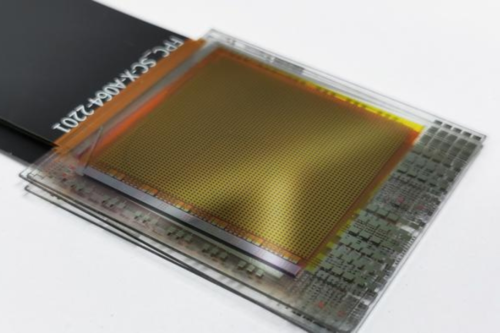
Kovalenko's team were able to demonstrate this a few years ago, initially with individual oversized pixels made of millimeter-large single crystals. Now, they have built two fully functional thin-film perovskite image sensors. “We are developing the technology further from a rough proof of principle to a dimension where it could actually be used,” says Kovalenko.
Tests on the prototypes (which differ in their readout technology) show the sensors are more sensitive to light, more precise in colour reproduction and can offer a significantly higher resolution than conventional silicon technology. The fact that each pixel captures all the light also eliminates some of the artifacts of digital photography, such as demosaicing and the moiré effect.
Consumer digital cameras are not the only application for perovskite image sensors. Due to the material's properties, they can be used for applications such as machine vision and hyperspectral imaging, by controlling the wavelength range absorbed by each layer.
“With perovskite, we can define a larger number of colour channels that are clearly separated from each other,” notes co-author Sergii Yakunin from Kovalenko's team. Silicon, with its broad absorption spectrum, requires numerous filters and complex computer algorithms. “This is very impractical even with a relatively small number of colours,” Kovalenko sums up. Hyperspectral image sensors based on perovskite could be used in medical analysis or in automated monitoring of agriculture and the environment, for example.
Next, the researchers want to further reduce the size and increase the number of pixels in the sensors. Their two prototypes have pixel sizes between 0.5 and 1mm. Pixels in commercial image sensors fall in the micrometer range. “It should be possible to make even smaller pixels from perovskite than from silicon,” says Yakunin. The electronic connections and processing techniques need to be adapted for the new technology.
“Today's readout electronics are optimised for silicon. But perovskite is a different semiconductor, with different material properties,” says Kovalenko. However, the researchers are convinced that these challenges can be overcome.


