Strain modulation techniques for enhancing LED efficiency
By promoting the heteroepitaxy of high-efficiency LEDs in the UV and the red, strain modulation is accelerating the development of III-nitride optoelectronics.
BY XINQIANG WANG FROM PEKING UNIVERSITY
GaN and its related alloys are continuing to attract tremendous attention in optoelectronics due to their excellent material properties. Strengths of these III-nitride semiconductors include a continuously tuneable bandgap, high electron mobility, superior radiation resistance, and excellent thermal stability. Such characteristics make this materials system ideal for producing a broad range of devices – and in particular light emitters, such as LEDs and lasers – that can serve in many different applications.
Within the III-nitride optoelectronic industry, the most notable triumph is the development of the InGaN-based blue LED. This device has revolutionised solid-state lighting, creating a market that’s worth tens of billions of dollars per annum and making significant contributions to global energy conservation and carbon reduction. Beyond lighting, the applications of III-nitride optoelectronics are diversifying. Currently, this expansion is focusing more and more on AlGaN alloys and high-indium-content InGaN alloys, materials that are enabling technologies such as UV light sources and microLED displays. There is growing demand for more efficient AlGaN-based UV LEDs and InGaN-based red LEDs, a pair of goals driving much progress.

Figure 1. The application fields for III-nitride optoelectronics are expanding to AlGaN alloys and high-indium-content InGaN alloys, such as UV light sources and microLED displays.
Lattice strain challenges
Compared with blue LEDs, those emitting in the red and UV are held back by greater strain in the active region. This gets more severe when increasing the gallium content in AlGaN-based UV LEDs, and increasing the indium content in InGaN red LEDs. In both cases, the strain, which degrades crystal quality, stems from differences in the lattice mismatch and the thermal expansion of the active layers and the substrate.
With AlGaN-based UV LEDs, lattice mismatch between the AlGaN layers and AlN templates generates compressive stress in the AlGaN films, leading to high dislocation densities and surface roughening in the active region. Due to these impediments, there is a reduction in the efficiency and the stability of the devices.
Similarly, for InGaN-based red LEDs, incorporating more indium results in a significant lattice strain and ultimately poor crystal quality. When these weaknesses arise, quantum efficiency plummets,
the emission peak broadens, and the emitter is plagued by a severe efficiency droop. Compounding these issues, lattice strain also causes substantial wafer bowing, particularly in LEDs grown on large-sized substrates. This deformation threatens to lead to non-uniform emission wavelengths across the wafer, and process challenges during chip fabrication.
The key to addressing these challenges is strain modulation. By carefully managing strain between the epitaxial structures and substrates, it is possible to improve the crystalline quality of the materials and enhance the overall performance of III-nitride optoelectronic devices.
Our team at Peking University is employing this strategy. By adopting this approach, we are making significant strides in improving AlGaN/AlN and InGaN/GaN systems, a critical step to increasing the efficiency of AlGaN-based UV LEDs and InGaN-based red LEDs.

Figure 2. The InGaN/GaN and AlGaN/AlN systems face similar issues of compressive stress, because both involve incorporating larger atoms into a host lattice composed of smaller atoms, such as embedding indium into GaN or gallium into AlN.
AlGaN strain strategies
For AlGaN UV LEDs, which are typically grown on AlN templates, AlGaN strain-modulation strategies aim to mitigate the compressive stress. This can be realised by adjusting the strain state of the AlN template, and by incorporating a strain-modulation buffer layer.
We alleviate the compressive stress in our AlN templates by high-temperature annealing, in the range 1600 °C to 1800 °C. This annealing step enhances the recrystallisation of AlN, and improves the in-plane orientation consistency of AlN columns, which are usually fabricated by physical vapour deposition. After high-temperature annealing, the dislocation density within our AlN templates is significantly reduced, ensuring improved crystal quality.
Further gains are realised by applying oxygen plasma irradiation to the sapphire substrate prior to AlN deposition, with this process improving the surface morphology of the high-temperature annealed AlN templates.
According to atomic force microscopy measurements over a 2 µm by 2 µm area, our 50 nm-thick high-temperature-annealed AlN template has a root-mean-square roughness of approximately 0.2 nm. We have also evaluated the quality of our templates with X-ray diffraction rocking curves, obtaining values for the full-width at half-maximum for the (002) and (102) planes of 51 arcsecs and 140 arcsec, respectively. These very low values highlight the superior quality of our high-temperature-annealed AlN templates, compared with conventional AlN templates.
Note that we have also shown that by adjusting the thickness of our templates, we can gradually shift the strain state of our AlN films from compressive to tensile. This ‘lever’ allows us to significantly improve our surface morphology, and enhance the overall performance of our AlGaN-based UVC LEDs that we grow on this foundation.

Figure 3. The strain modulation strategy of AlGaN-based
UV LEDs can be implemented by either adjusting the strain state of the AlN
template or by introducing a strain-modulation buffer layer.
The AlGaN UVC LEDs that we have fabricated on our ultra-thin, high-temperature-annealed AlN templates exhibit excellent luminous efficiency and reliability. By optimising the strain state and controlling the crystalline quality of this engineered platform, our 0.5 mm by 0.5 mm AlGaN UVC LED chip produces a wall-plug efficiency of 3.95 percent at a peak wavelength of 278 nm. After 1,000 hours of aging, the light output power remains at 91 percent of its initial value.
What’s also appealing with this approach is that compared with traditional UVC-LED structures, we trim the epitaxial cost of this emitter by 60 percent, thanks to the use of our ultra-thin template. This significant cost saving makes our form of UVC LED more economically feasible for commercial production.
Another option for effective strain modulation in AlGaN UV LEDs involves the use of AlN templates grown on nano-patterned sapphire substrates. Introducing nano-scale patterns results in a periodically arranged array of holes or pillars in the AlN films during the early growth stages. When these AlN nanostructures coalesce, they provide a mechanism for strain modulation. Influencing the stress state within the AlN film are a number of factors, including the type and size of the pattern. We have found that using hole-textured nano-patterned sapphire substrates induces greater tensile stress during the coalescence of AlN nanostructures, compared with pillar-textured nano-patterned sapphire substrates.
For the hole-textured nano-patterned sapphire substrates, the diameter of the hole governs the stress state of the AlN template. As the size of the holes decreases from 750 nm to 550 nm, the AlN film transitions from a compressive to a tensile stress state. The nature of this stress influences surface morphology and the performance of AlGaN-based UV LEDs. By optimising the hole diameter – it is ideally 600 nm – we strike a balance between promoting a smoother surface morphology for AlGaN-based UV LEDs, and minimising crack formation in the AlN template.
We have found that the opportunity to fine-tune the hole diameter is especially beneficial for the development of high-performance AlGaN-based UV LED chips. Using hole-textured nano-patterned sapphire substrates, we have produced AlGaN-based UVB LED chips with dimensions of 0.5 mm by 0.5 mm that produce a wall-plug efficiency of 3.27 percent at a peak wavelength of 303.6 nm, and a light output power of 57.6 mW at 800 mA.
The devices also have promising reliability, with an L70 lifetime of approximately 7800 hours, and the light output power retaining 83 percent of its initial value after 1,000 hours of aging. Another significant result with our hole-textured nanopatterned sapphire technology is a wall-plug efficiency exceeding 6.5 percent for our UVC LED chips. Taken together, these results highlight the significant potential of this approach for advanced optoelectronic applications.
It’s also possible to use a strain modulation buffer layer to manage the strain in AlGaN-based UV LEDs. One promising approach involves an AlN transition layer, comprising a three-dimensional (3D) island-like AlN layer, followed by a two-dimensional (2D) continuous AlN recovery layer. Through homo-epitaxial growth of the 3D-2D transition layer on our high-temperature-annealed templates, we can ensure that the 3D-grown AlN islands maintain a consistent c-axis orientation. We observe that during the 2D AlN recovery process, tensile strain is introduced via grain coalescence, successfully converting the initial compressive strain into tensile strain. This is a valuable transformation, enhancing the surface morphology of our AlGaN-based UV LEDs. Drawing on this benefit, we have produced crack-free 4-inch UVC-LED wafers with an outstanding performance. Devices with dimensions of 0.25 mm by 0.5 mm deliver an output power of 14 mW at 275 nm, under a forward current of 100 mA. This success underscores the significant potential of the 3D-2D AlN transition layer for advancing the performance and scalability of UVC LEDs.

Figure 4. Lattice and thermal mismatches lead to compressive strain in heteroepitaxial GaN films on sapphire, while grain boundary coalescence induces tensile strain.
InGaN strain strategies
The challenges faced by engineers developing and producing AlGaN-based UV LEDs also impede the progress of the pioneers of InGaN-based red LEDs. In both cases, compressive stress is an issue, arising from the incorporation of larger atoms into a host lattice composed of smaller atoms – such as indium into GaN or gallium into AlN.
For InGaN-based red LEDs, the strain-related issues are more severe than those for AlGaN-based UV LEDs, due to the greater lattice mismatch between InGaN and GaN. Compressive stress from the underlying GaN layers limits indium incorporation during the epitaxy of high-indium-content InGaN materials, leading to poor crystalline quality, phase separation, surface segregation, and other detrimental effects.
According to theoretical calculations, indium incorporation is more favourable when the GaN lattice is under tensile strain. Unfortunately, such conditions do not occur during heteroepitaxy on substrates such as sapphire, as this tends to induce compressive strain in GaN films, due to lattice and thermal mismatches. Consequently, the primary strategy for strain management in InGaN-based red LEDs involves either relieving compressive strain or inducing tensile strain in the underlying heteroepitaxial GaN films.
To effectively modulate the strain in heteroepitaxial GaN films, we have turned to a composite buffer structure, grown on sapphire, that leverages the tensile stress generated during grain coalescence. Our composite buffer consists of a sputtered AlN nucleation layer, followed by a low-temperature GaN layer, grown by MOCVD. The sputtered AlN nuclei exhibit excellent c-axis orientation, while the low-temperature GaN layer forms numerous 3D GaN islands, originating from these AlN nuclei and separated by grain boundaries. During subsequent growth, adjacent GaN islands coalesce as they seek to minimise surface-free energy, which outweighs the formation energy of the grain boundaries. This coalescence process stretches the crystallites, generating tensile stress within the low-temperature GaN buffer layer. This tensile stress significantly enhances indium incorporation in InGaN-based red LEDs, addressing a key challenge associated with compressive strain in high-indium-content materials.
Unfortunately, simply managing strain in the underlying GaN layer is insufficient to ensure high-performance InGaN-based red LEDs, due to the significant lattice mismatch in these devices. What’s also needed is additional strain modulation, realised through the structural design of the active region.
Our research reveals a substantial deterioration in the quality of InGaN-based red quantum wells when two or more are grown consecutively. To address this, one can introduce structures such as InGaN/GaN superlattices that provide strain modulation in the high-indium-content active region. This approach significantly mitigates the degradation of epitaxial quality.
As well as adopting this approach, we have developed a periodic quantum-well structure that feature alternating cycles of high- and low-indium compositions. Our experimental results confirm that this design significantly improves the performance of InGaN red LEDs.

Figure 5. High-efficiency UVC, UVB, and red LEDs have been realised by implementing adaptive strain-modulation strategies tailored to the AlGaN/AlN and InGaN/GaN systems.
To tackle indium surface segregation caused by stress, and to enhance the sharpness of the active region interfaces, we have introduced an AlGaN/GaN confinement layer that follows the InGaN-based red quantum well. Note that we have found that it is crucial to optimise the growth temperature of this confinement layer, as this ensures uniform confinement of indium atoms within the wells. Our investigations show that the confinement layer plays a pivotal role in enhancing the electroluminescence intensity of InGaN-based red LEDs.
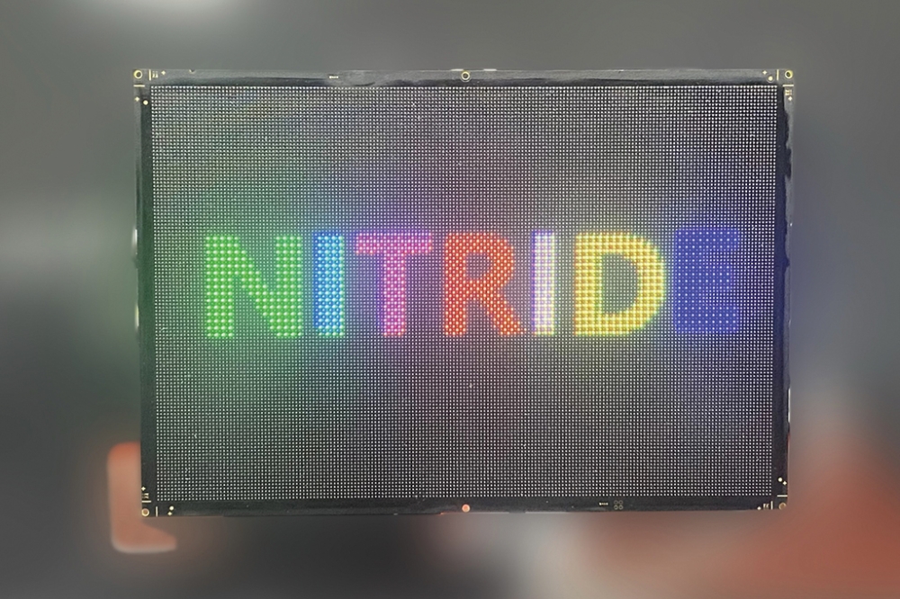
Deploying these innovative strain-modulation strategies has enabled us to produce promising InGaN-based red LEDs on 4-inch sapphire substrates. Our InGaN-based red mini-LED chips operate with a working current density of around just 0.5 A cm-2, have an external quantum efficiency of about 7.4 percent, and have a peak wavelength of around 629 nm. We have successfully integrated these chips into a full-colour nitride-based mini-LED display, covering 74.1 percent of the Rec. 2020 colour gamut. These results underscore the tremendous potential of InGaN-based red mini/microLEDs in high-resolution, full-colour advanced display applications.
By systematically exploring strain modulation strategies for both the AlGaN/AlN and InGaN/GaN systems, we have demonstrated high-efficiency LEDs emitting in the UVC, UVB, and red spectral domains. This success, realised by precisely tailoring the strain through substrate patterning, growth mode transitions, and epitaxial structure design, highlights the critical role of strain engineering in III-nitride semiconductor heteroepitaxy and its significance for advancing III-nitride optoelectronics.