Loading...
News Article

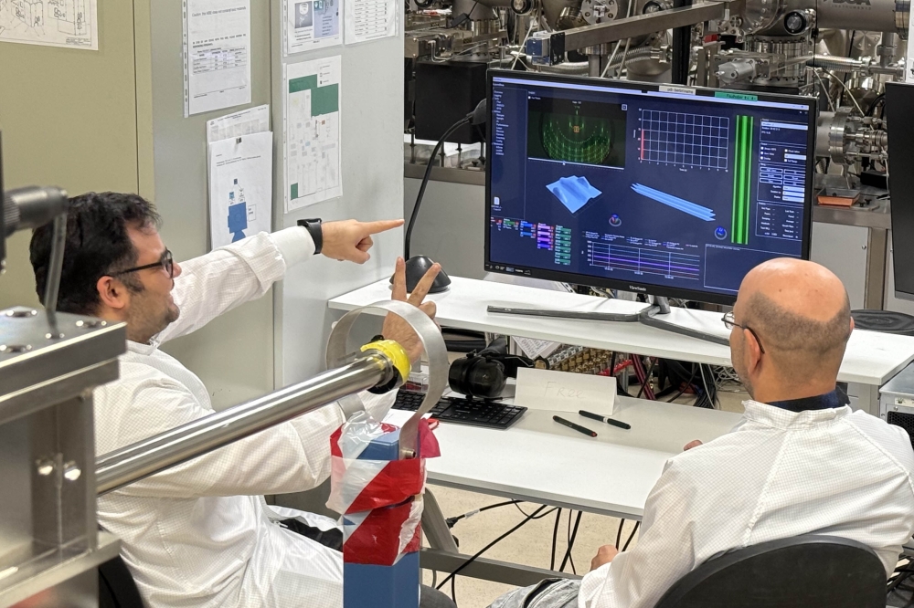
US SiC R&D facility celebrates topping out

News

21,760-square-foot SiC prototyping, testing and fabrication facility in Arkansas reaches first milestone

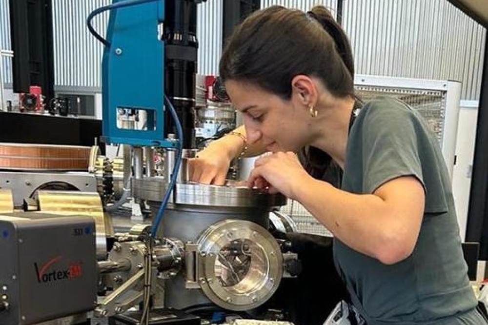
The University of Arkansas has celebrated a milestone with the topping-out of the Multi-User SiC Research and Fabrication Facility.

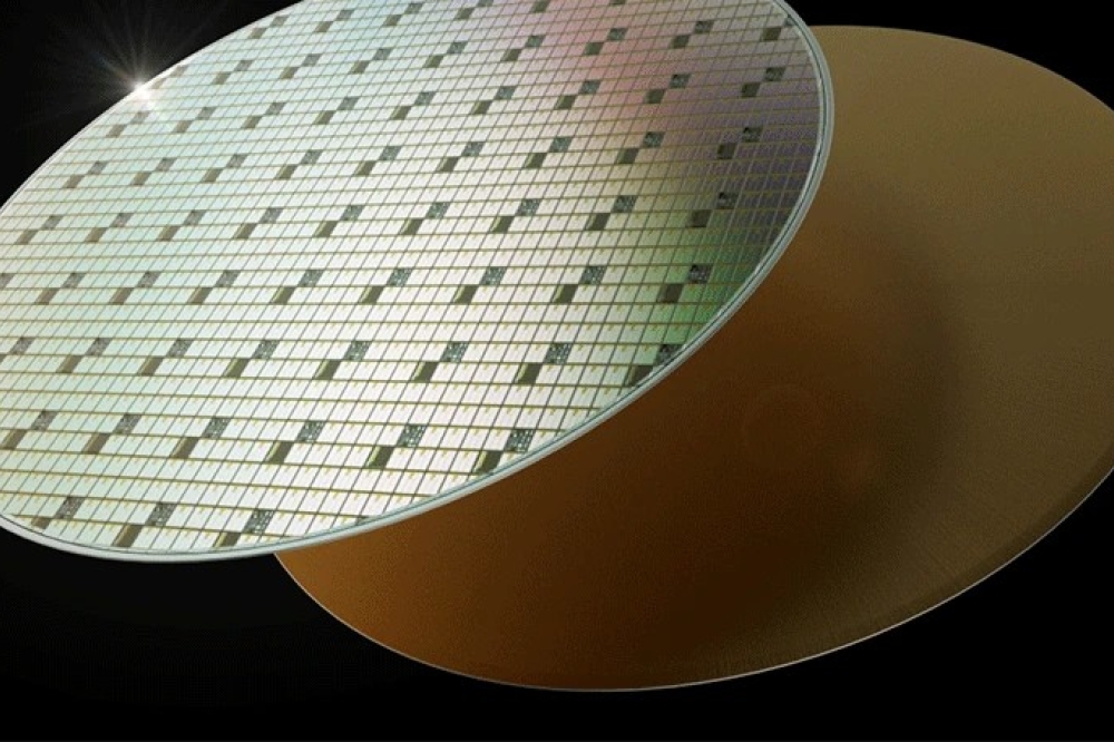
The new semiconductor facility will enable the federal government – via national laboratories – businesses of all sizes and other universities to prototype with SiC, a capability that does not presently exist elsewhere in the United States.

Work at the facility is intended to bridge the gap between traditional university research and the needs of private industry. The aim is to accelerate technological advancement by providing a single location where chips can go from developmental research to prototyping, testing and fabrication.

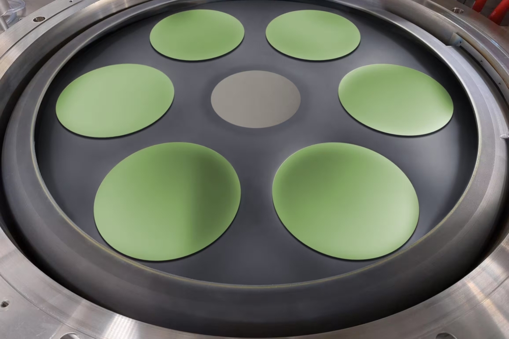
The 21,760-square-foot facility, located next to the National Center for Reliable Electrical Power Transmission at the Arkansas Research and Technology Park, will feature approximately 8,000 square feet of clean rooms for fabrication and testing.

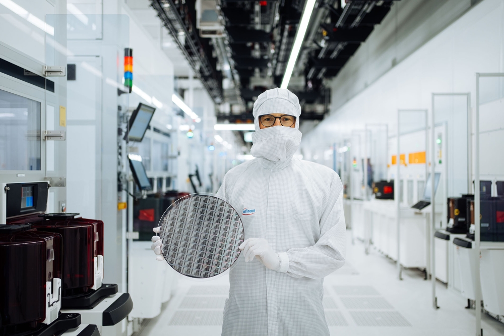
Education and training within the facility will also accelerate workforce development, helping supply the next generation of engineers and technicians in semiconductor manufacturing.

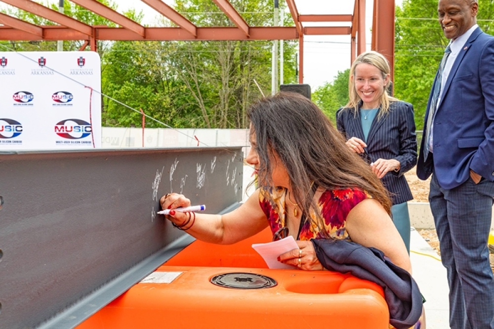
Pictured above: From left, Kim Needy, dean of the College of Engineering, signs a beam while Margaret Sova McCabe, vice chancellor for research and innovation, and Chancellor Charles Robinson observe.

Tariff uncertainty weighs on displays
Flexible perovskite/CIGS tech reaches 23.64% efficiency
IQE and X-FAB sign GaN power collaboration
Riber reports solid growth in sales and earnings
How to make green ZnSeTe QD-LEDs brighter
Korean team makes novel flexible ammonia sensor
Optimising green LEDs for near-eye applications
MoD to put £200m into UK compound semi fab
EU invests €15M to help firms use photonics
ST and Innoscience sign GaN deal
Lumentum shows InP advances at OFC
A step towards higher DUV LED efficiency
Quantum Science achieves ISO 9001:2015 certification
Ascent wins order for power-beaming module
Navitas Partners with Great Wall for 400V-DC power
SemiQ supplies SiC MOSFET modules for EV battery cell cyclers
Coherent and Keysight collaborate on 200G/lane multimode VCSEL tech
Lumentum and Marvell exhibit integrated 450G optical interface
Marktech announces new MWIR LEDS
Imec identifies stable range for GaN MISHEMTs in RF PAs
Polar Light completes $3.4m funding round
Lynred launches advanced thermal imaging modules
Altum RF expands Sydney design centre
Sivers announces partnership with O-Net
Ayar Labs unveils first UCIe optical chiplet
Aixtron delivers InP tool to Nokia
WHU-USTC team demo novel GaN chip temperature monitoring
Phlux lands £9m to take InGaAs sensors to next level
4-inch gallium oxide facility established in Swansea
Mazda and Rohm collaborate on automotive GaN
University of South Carolina chooses MOCVD tool from TNSC
Wolfspeed appoints new CEO amidst funding crisis
×
Search the news archive

To close this popup you can press escape or click the close icon.
Logo
x
Logo
×
Register - Step 1

You may choose to subscribe to the Compound Semiconductor Magazine, the Compound Semiconductor Newsletter, or both. You may also request additional information if required, before submitting your application.


Please subscribe me to:


You chose the industry type of "Other"

Please enter the industry that you work in:
 
x
Adblocker Detected
Please consider unblocking adverts on this website