
Cooling RF GaN HEMTs with all-around diamond
Engineers from Stanford University are claiming to have broken new ground with the first post-process diamond integration of a GaN HEMT. It is argued that this approach, which wraps a 150 mm N-polar GaN MIS-HEMT in diamond, will provide a valuable platform for the thermal management of X-band GaN HEMTs using diamond heat spreaders.
This team’s work is one of a number of approaches, developed over many years, for addressing self-heating in GaN HEMTs – this is an issue that impacts this device’s performance and reliability.
Many attempts to reduce self-heating involve trimming the thermal boundary resistance to the channel of the HEMT via backside integration of heat spreaders. Previous efforts have included growing GaN HEMT stacks on diamond substrates, transferring the substrate from sapphire to copper, and adding copper-filled micro-trenches.
One downside of all forms of backside integration is that the heat generated in the channel has to flow through the buffer and/or nucleation layers that tend to have a high thermal resistance.
To address this drawback, the team from Stanford integrates diamond on both the top and the sidewalls of the device’s active area, enabling a route for heat extraction that bypasses the high-resistance buffer and/or nucleation layers.
The team’s latest approach is its successor to its previous technologies, described as ‘diamond first’ and ‘gate first’.
According to team spokesman Srabanti Chowdhury, those predecessors – the diamond-first and the gate-first processes – offer promising advantages over other approaches, and are each suited to different integration strategies.
Offering insights into both of them, Chowdhury remarks: “In the diamond-first process, lithography for the gate and other device regions must be performed directly on the diamond surface, which can be challenging – particularly at sub-micron scales.”
He adds that in contrast, the gate-first process involves depositing diamond over a pre-defined gate structure, eliminating the need for gate lithography on diamond. Due to this, the gate-first process is the more manageable approach from a fabrication standpoint.
“However, the success of the gate-first approach hinges on the ability to grow diamond at sufficiently low temperatures to avoid degrading the electrical performance of the underlying gate stack,” says Chowdhury. “When this condition is met, diamond integration over the gate becomes feasible and attractive.”
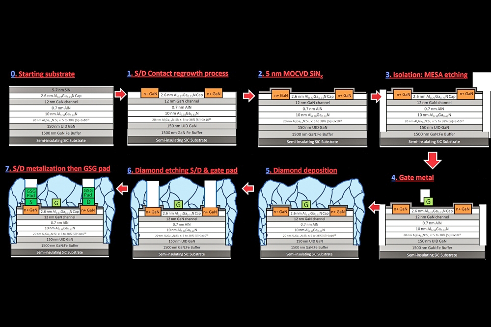
The team’s process, illustrated in the figure, begins with the formation of a GaN-on-SiC epistack by MOCVD, followed by the addition of source, gate and drain contacts, deposition of diamond, localised etching, and the addition of ground-signal-ground pads.
Chowdhury and co-workers have produced two forms of gate all-around HEMT, with diamond deposition at 500 °C and at 700 °C. “Growth at 700 °C is easier and more straightforward from a growth standpoint, but it is not practical for a gate-first process,” explains Chowdhury, who points out that this temperature exceeds the thermal budget of the gate stack. “In contrast, with a 500 °C or lower temperature growth process, safe integration is achievable without such risks.”
Devices produced using diamond deposition at 700 °C exhibit no gate modulation, due to a high gate leakage, stemming from the high growth temperature for diamond. Meanwhile, measurements on devices produced with diamond deposition at 500 °C reveal a threshold voltage of -8 V, an on-off ratio of 105, a peak transconductance of 190 mS mm-1, and a drain saturation current of 0.96 mA mm-1.
“Future research will focus on scaling this integration into larger device arrays and investigating long-term reliability under high-power operation,” says Chowdhury, whose plans also include exploring integration with alternative gate architectures and packaging schemes, to further improve thermal and electrical co-optimisation. “Ultimately, our goal is to develop a scalable, manufacturable thermal integration strategy that enables high-power density, thermally reliable GaN devices for X-band and beyond.”
Reference
R. Soman et al. Appl. Phys Express 18 046503 (2025)
Pictured above: Stanford’s latest approach to minimising self-heating of the channel enables the fabrication of an all-around diamond N-polar GaN HEMT.


