1200 V GaN monolithic power integration
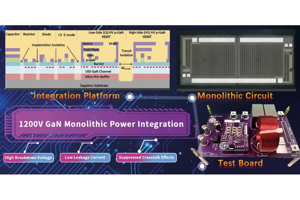
Sapphire substrates with ultra-thin buffer layers provide a foundation for fabricating systems offering 1200 V GaN-based monolithic power integration while suppressing crosstalk.
BY SHENG LI, SIYANG LIU AND WEIFENG SUN FROM SOUTHEAST UNIVERSITY AND TINGGANG ZHU FROM CORENERGY SEMICONDUCTOR
Our electrified world contains countless examples of energy conversion. Within this sector the GaN-based power device attracts extensive attention, thanks to its capability to switch high voltages at high speeds. However, there are concern associated with this wide bandgap technology. In power systems featuring GaN, inductive elements generate rings and spikes during switching, ultimately leading to an increase in fault risk.
One increasingly popular way to address this concern is to eliminate the parasitic inductive elements by turning to a monolithically integrated gate driver and half-bridge configuration. However, this approach is compromised, with state-of-art GaN based monolithic integration limited to 650 V. That’s far from ideal, given the rapid development of power electronic systems requiring power devices with a rated voltage above 1200 V.
The conventional foundation for GaN power devices is the silicon substrate. While it is low in cost and widely available, it is impaired by a conductivity that is to blame for the vertical breakdown and crosstalk in conventional 650 V GaN-on-silicon platforms. These are significant limitations, hampering efforts to increase the rated voltage of monolithic integration.
Progress demands a more radical approach, such as the one we are taking at Southeast University and CorEnergy Semiconductor. Our partnership is pioneering an ultra-thin buffer technology with shallow trench isolation on a sapphire substrate. Using this approach, we have realised a 1200 V monolithic half-bridge integration platform that supresses crosstalk.
Figure 1. (a) 1200 V E-mode GaN based monolithic half-bridge integration platform on sapphire. (b) Photos of trench isolation. (c) Key fabrication processes. (d) Scanning electron microscopy of 1200 V GaN-HEMT monolithic half-bridge integration.
Fabrication of our platform begins by loading sapphire substrates into an MOCVD reactor and depositing a 100 nm-thick undoped ultra-thin buffer, followed by a 300 nm-thick undoped GaN channel layer and a 15 nm-thick Al0.23Ga0.77N barrier layer ((see Figure 1(a)). This epitaxial structure is capped with a 100 nm-thick p-GaN cap layer, magnesium doped at a level of 2 × 1019 cm-3.
To produce devices from this epilayer, we define a trench with a dry etching process based on BCl3/Cl2 – this follows an implantation process (see Figure 1(b)). We suppress the influence of sidewall traps along the trench by surrounding it with an implantation area. Our other fabrication processes are consistent with those of a normal p-GaN HEMT (see Figure 1(c) for an overview of our key fabrication processes).
Our ultra-thin buffer technology allows us to realise wafer-level integration of high-voltage (HV) and low-voltage (LV) enhancement-mode p-GaN gate HEMTs with LV passive elements, including diodes, resistors, and capacitors. Undertaking shallow trench isolation by etching the ultra-thin buffer is a relatively easy process, which supresses crosstalk between high-side and low-side HV p-GaN HEMTs. Following etching, we fabricate our monolithic half-bridge circuits with gate buffers (see Figure 1(d)). The formation of our integration platform is relatively quick and material costs are low, making this an attractive technology for mass production.
Figure 2. (a) Blocking characteristics of a HV p-GaN HEMT. (b) Extracted blocking voltage with different gate-to-drain lengths (Lgd). (c) Terminal capacitances at different temperatures. (d) Double pulse test switching characteristics of the turn-on process. (e) Double pulse test switching characteristics of the turn-off process. (f) Comparisons of the dynamic on-resistance between GaN-on-sapphire and GaN-on-silicon HEMTs.
Ultra-thin buffers
It is essential to eliminate the traps caused by heteroepitaxy, as they threaten to impair mobility in the GaN channel. With conventional GaN-on-silicon HEMTs, traps are typically suppressed by combining a nucleation layer with a thick buffer layer. Switching to a sapphire substrate reduces lattice mismatch with the GaN-based epilayers and enables a 100 nm-thick undoped ultra-thin buffer layer to suppress traps from the substrate and ensure a high-quality GaN channel.
Additional attractive features of our architecture are that it provides a low lateral leakage current and a high lateral breakdown voltage, thanks to the ease of depletion of the thin buffer and the channel under the gate region. What’s more, due to the isolated sapphire substrate, the vertical blocking voltage can be increased without needing a thick buffer.
Electrical measurements underscore the superior blocking characteristics of our HV p-GaN HEMTs, which benefit from an ultra-thin buffer. We have realised a blocking voltage of more than 1400 V for a gate-to-drain length of just 10 µm in our p-GaN HEMT (see Figure 2(a) and 2(b)). This equates to 140 V/μm, which is 140 percent of that of a SOI-based p-GaN HEMT. To ensure a healthy safety margin, for devices rated at 1200 V we propose a gate-to-drain length of 22 µm – this geometry offers a blocking voltage of over 2300 V.
Other encouraging results from our HV p-GaN HEMT include its capability to withstand transient voltages higher than 1400 V for 10 ms, an attribute that helps improve reliability when an overvoltage event occurs. At a drain-source voltage of 1200 V, the drain leakage current is less than 100 pA/mm and 100 nA/mm at 25 °C and 175 °C, respectively. That’s a leakage current level about two orders of magnitude smaller than that for GaN-on-silicon HEMTs. For those devices, the leakage current at high voltages rapidly increases with drain voltage, due to parasitic channels and vertical leakage caused by the conductive substrate. Our devices offer an extremely low drain leakage current, due to the isolated substrate and the undoped ultra-thin buffer, and they benefit from successful suppression of the parasitic channel at the interface between the epitaxial layers and the substrate.
We have also evaluated the dynamic electrical performance of our HV p-GaN HEMT (see Figure 2(c)-(e)). At high temperatures there is variation in terminal capacitances, but the influence on switching speed can be neglected, according to double pulse test results. Values for the turn-on delay time and rise time indicate fast switching speeds, even at 800 V. The turn-off delay and fall times are longer than they might be, due to a large external turn-off resistance of 30 Ω and a small switching current 1.5 A.
Figure 3. Crosstalk evaluation: (a) test setups, (b) crosstalk of two separated GaN-on-silicon devices with the substrate connected together, (c) no crosstalk observed on GaN-on-sapphire half-bridge devices.
A big concern for all power GaN HEMTs is the dynamic on-state resistance, with higher values increasing conduction loss and junction temperature. We have used a test circuit to provide a highly accurate comparison of the dynamic on-state resistance of conventional GaN-on-silicon HEMTs and our HV p-GaN HEMTs. This investigation revealed that our devices have the upper hand in this regard, thanks to a reduction in the general trap activation energy, resulting from the undoped ultra-thin buffer technology (see Figure 2 (f)).
Trench isolation
The monolithic integration of GaN power systems on a single chip has much appeal. There is the promise of suppressed parasitic inductance, reduced die size and greater design flexibility.
However, it’s far from easy to fulfil this dream with GaN-on-silicon, due to the common conductive silicon substrate. There are reports that when the high side (HS) transistor and low side (LS) transistor are built on this conventional platform, the system suffers from back-gating and crosstalk effects, coupled through the common silicon substrate.
A number of substrate technologies have been proposed to address this issue, such as Qromis’ engineered platform, as well as silicon-on-insulator substrates and engineered bulk silicon substrates. However, for all these platforms the rated voltage is restricted to no more than 650 V, due to vertical breakdown. With all these platforms, it may be tempting to try and increase the vertical breakdown voltage by introducing a thicker buffer, but this is not practical, due to wafer warpage, traps and high costs.
Offering a far better way forward is our ultra-thin buffer technology, based on insulated sapphire substrates. Crosstalk effects are avoided with shallow trench isolation, realised by etching the ultra-thin buffer layer (see Figure 1 (b)). With this architecture, the breakdown voltage of the trench isolation structure exceeds 3000 V at 175 °C, while maintaining an acceptable increase in leakage current and thus ensuring safe isolation between HS and LS devices. Another strength of this design is that it provides effective suppression of the substrate biasing effect, due to the insulated substrate withstanding the voltage drop between the electrodes and substrate.
To characterise the crosstalk between the HS and LS devices, we apply a small drain-source voltage to the LS p-GaN HEMT, and then apply a pulsed high-voltage stress to the HS devices and substrate (see Figure 3(a)). Due to high-voltage stress, trapping occurs in the LS p-GaN HEMT during the stress stage. We are then able to quickly monitor crosstalk after the stress stage.
For the conventional GaN-on-silicon platform, we observe a build-up in the dynamic positive voltage between the HS source and the LS source when the HS in ‘on’ and the LS is ‘off’. Following this, there is a dynamic positive substrate-to-source stress voltage during the transition to HS ‘off’ and LS ‘on’ that drives electrons injection into the buffer of the LS p-GaN HEMT. When the half-bridge circuit switches so that it is also in this phase – that is, HS ‘off’ and LS ‘on’ – electrons trapped in the buffer region of the LS p-GaN HEMT cannot be emitted in time, and tend to partially deplete the 2DEG channel of the LS p-GaN HEMT, resulting in la ower drain current. That’s not the case for our platform, however, thanks to suppression of crosstalk between HS and LS HV p-GaN HEMTs, due to shallow trench isolation into the sapphire substrate.
The superiority of our platform is highlighted by our measurements of the drain current of a conventional GaN-on-silicon device and our proposed half-bridge device (see Figure 3(b) and 3(c)). Our results uncover obvious crosstalk in GaN-on-silicon devices at a 400 V stress voltage at room temperature, and demonstrate effective elimination of crosstalk by shallow trench isolation with our GaN-on-sapphire platform, even at a 900 V stress voltage and a temperature of 175 °C. These results indicate that trench isolation enables high-temperature operation of a monolithic GaN half-bridge device at a high voltage – the aim is 1200 V.
Figure 4. Boost converter performances: (a) experimental printed circuit board, (b) circuit, (c) 800 V/1 MHz output waveforms.
Monolithic ICs
To evaluate the performance of our 1200 V monolithic half-bridge circuit, we have constructed a boost converter (see Figure 4(a) and 4(b)). The output results, shown in Figure 4(c), reveal that our converter can operate under 800 V/1 MHz conditions at 175 °C.
These results indicate that our proposed GaN-on-ultra-thin buffer technology is a compelling candidate for producing GaN devices for high-temperature, high-voltage power systems (see Table 1 for a comparison of our technology and that involving other foundations).
Table 1. Comparison of p-GaN HEMT based monolithic integration with high blocking voltages
Adding to the appeal of our approach are cheap substrates and simple epitaxy, merits that slash costs and enable GaN HEMTs to target a wider range of applications. They include electric vehicles and renewable energy markets, both of which would benefit from our proposed monolithic half-bridge integration platform that combines high temperatures and high voltages with suppressed cross talk.


