Turning up the heat on GaN

Researchers shed light on GaN properties that could be used in extremely hot environments
On the surface of Venus, temperatures can climb to 480 degC, which is one reason scientists have not yet been able to send a rover to the planet’s surface (silicon-based electronics can’t operate in such extreme temperatures for an extended period of time).
For high-temperature applications like Venus exploration, researchers have recently turned to GaN. Now in a new paper published in Applied Physics Letters, which is part of a multiyear research effort, a team of scientists from MIT and elsewhere have sought to answer key questions about the material’s properties and performance at extremely high temperatures.
They studied the impact of temperature on the ohmic contacts in a GaN device, and found that extreme temperatures didn’t cause significant degradation to the GaN material or contacts. They were surprised to see that the contacts remained structurally intact even when held at 500 degC for 48 hours.
Understanding how contacts perform at extreme temperatures is an important step toward the group’s next goal of developing high-performance transistors that could operate on the surface of Venus. Such transistors could also be used on Earth in electronics for applications like extracting geothermal energy or monitoring the inside of jet engines.
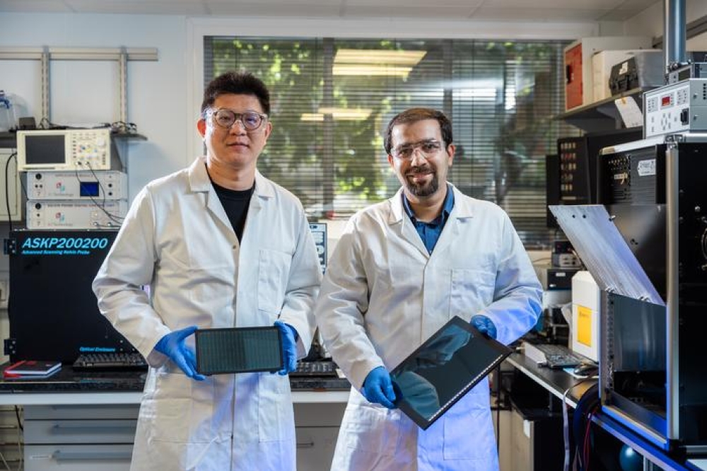
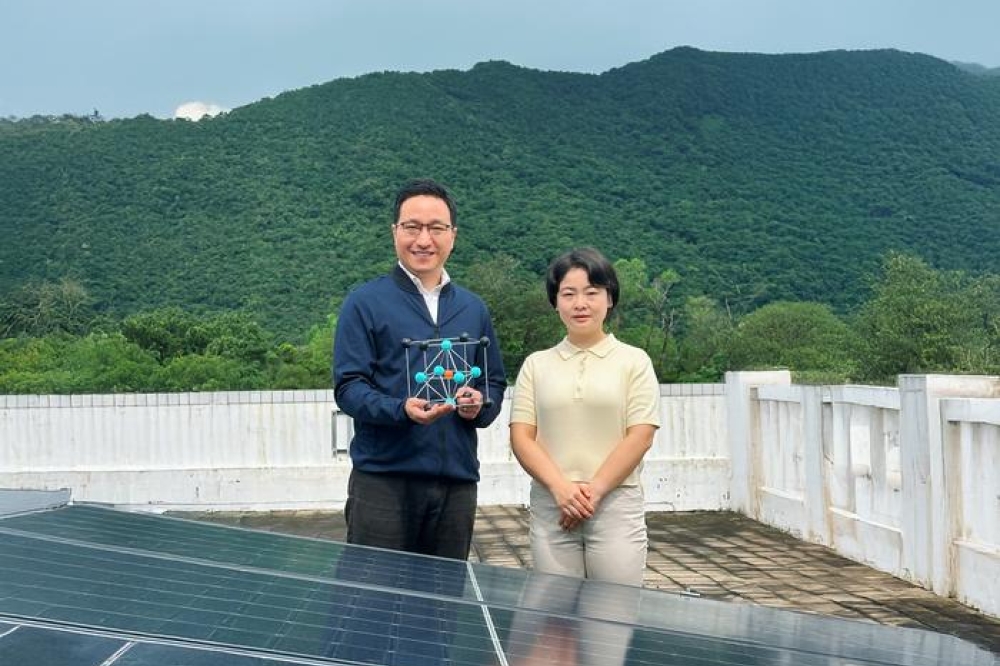
“Transistors are the heart of most modern electronics, but we didn’t want to jump straight to making a GaN transistor because so much could go wrong. We first wanted to make sure the material and contacts could survive, and figure out how much they change as you increase the temperature. We’ll design our transistor from these basic material building blocks,” says John Niroula, an electrical engineering and computer science (EECS) graduate student and lead author of the paper.
Turning up the heat
While GaN has recently attracted much attention, the material is still decades behind silicon when it comes to scientists’ understanding of how its properties change under different conditions. One such property is resistance, the flow of electrical current through a material.
A device’s overall resistance is inversely proportional to its size. But devices like semiconductors have contacts that connect them to other electronics. Contact resistance, which is caused by these electrical connections, remains fixed no matter the size of the device. Too much contact resistance can lead to higher power dissipation and slower operating frequencies for electronic circuits.
“Especially when you go to smaller dimensions, a device’s performance often ends up being limited by contact resistance. People have a relatively good understanding of contact resistance at room temperature, but no one has really studied what happens when you go all the way up to 500 degrees,” Niroula says.
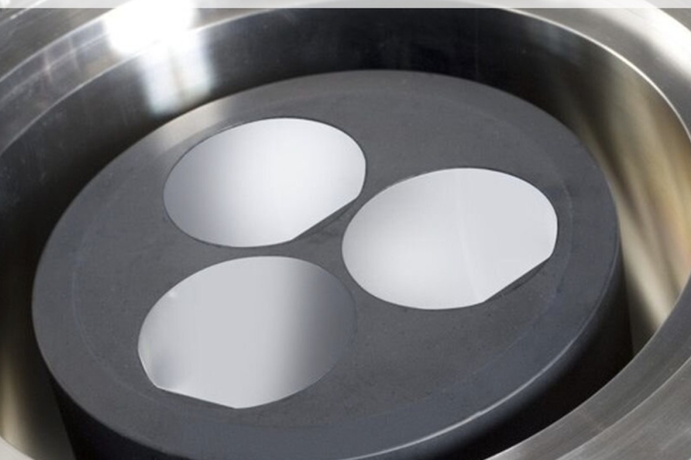
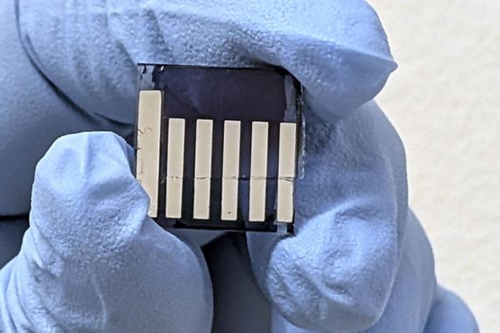
For their study, the researchers used facilities at MIT.nano to build GaN devices known as transfer length method structures, which are composed of a series of resistors. These devices enable them to measure the resistance of both the material and the contacts.
They added ohmic contacts to these devices using twocommon methods. The first involves depositing metal onto GaN and heating it to 825 degC for about 30 seconds, a process called annealing.
The second method involves removing chunks of GaN and using a high-temperature technology to regrow highly doped GaN in its place, a process led by Rajan and his team at Ohio State. The highly doped material contains extra electrons that can contribute to current conduction.
“The regrowth method typically leads to lower contact resistance at room temperature, but we wanted to see if these methods still work well at high temperatures,” Niroula says.
They tested devices in two ways. Their collaborators at Rice University, conducted short-term tests by placing devices on a hot chuck that reached 500 degCs and taking immediate resistance measurements. At MIT, they conducted longer-term experiments by placing devices into a specialised furnace the group previously developed. They left devices inside for up to 72 hours to measure how resistance changes as a function of temperature and time.
Microscopy experts at MIT.nano (Aubrey N. Penn) and the Technology Innovation Institute (Nitul S. Rajput) used state-of-the-art transmission electron microscopes to see how such high temperatures affect GaN and the ohmic contacts at the atomic level.
“We went in thinking the contacts or the GaN material itself would degrade significantly, but we found the opposite. Contacts made with both methods seemed to be remarkably stable,” says Niroula.
While it is difficult to measure resistance at such high temperatures, their results indicate that contact resistance seems to remain constant even at temperatures of 500 degrees, for around 48 hours. And just like at room temperature, the regrowth process led to better performance.
The material did start to degrade after being in the furnace for 48 hours, but the researchers are already working to boost long-term performance. One strategy involves adding protective insulators to keep the material from being directly exposed to the high-temperature environment.
Moving forward, the researchers plan to use what they learned in these experiments to develop high-temperature GaN transistors.
This work was funded, in part, by the US Air Force Office of Scientific Research, Lockheed Martin, the Semiconductor Research Corporation through the US Defense Advanced Research Projects Agency, the US Department of Energy, Intel, and the Bangladesh University of Engineering and Technology.