FETs: A mighty marriage
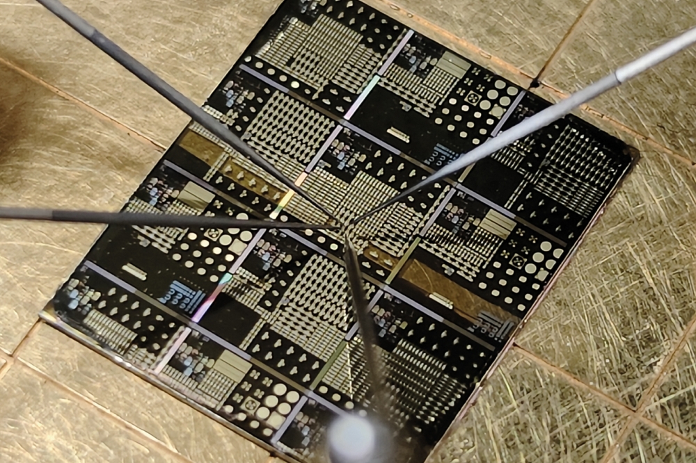
A monolithic architecture combines the complementary merits of GaN lateral heterojunctions and SiC vertical power devices.
BY SIRUI FENG, ZHEYANG ZHENG AND KEVIN J CHEN FROM THE HONG KONG UNIVERSITY OF SCIENCE AND TECHNOLOGY
The revolution in power electronics is well underway. Following decades of research and development, sales of SiC and GaN devices are now soaring, and will continue to climb for many years to come. Their commercialisation is creating a pair of multi-billion-dollar markets: GaN is now extensively deployed in consumer electronics, such as fast and compact chargers for the latest smartphones and laptops; and SiC is grabbing significant market share in photovoltaic inverters, as well as motor drives for electric vehicles.
Further development of GaN and SiC power electronics technologies will inevitably lead to intense competition between these two classes of device. It’s a battle that will be fought most fiercely in power range that spans 1 kW to 100 kW, due to the overlap of the power handling capabilities of GaN and SiC. While both are improving, due to efforts to increase the capability of the GaN and the SiC power transistor, is it possible that their marriage could deliver an even greater performance?
Friends or foes?
To answer this crucial question, let’s begin by taking a comparative look at the prevailing structures of the dominant GaN and SiC power devices, as summarised in Table 1. For this evaluation, it makes sense to consider the most popular GaN and SiC power devices, namely the GaN HEMT and the SiC power MOSFET (see Figure 1).
The GaN HEMT is a lateral device with small terminal capacitances. It is renowned for its high mobility, typically 2000 cm2 V-1 s-1, associated with the polarisation-induced two-dimensional electron gas (2DEG) at the AlGaN/GaN hetero-interface. The small capacitance and high mobility ensure that this device is very fast. To provide enhancement-mode operation to satisfy the fail-safe requirement, a non-negotiable in power electronics applications, this class of HEMT incorporates a p-type GaN gate. As well as enjoying volume adoption in compact fast chargers, this design is under intensive development for industrial and automotive applications.
In contrast to the GaN HEMT, the SiC MOSFET has a vertical geometry, leading to a relatively large conduction volume. It is possible to manufacture a variety of p-n junctions under the MOS channel using mature and robust ion-implantation and epitaxy techniques. These processes produce devices with a high blocking voltage and avalanche capability, traits that have garnered widespread deployment in high-power applications, such as electric vehicles and photovoltaic inverters.
However, while the GaN HEMT and the SiC MOSFET have had unquestionable market success, this should not obscure their issues. For both devices, the full potential is still to be unleashed.
One of the significant weaknesses of the lateral GaN HEMT is that scaling of the voltage rating compromises the bang-per-buck, due to an increased terminal spacing that occupies a larger area. Another issue is that this class of transistor has a small conduction volume, with the 2DEG channel just a few nanometres thick. The small conduction volume impedes the current handling and the thermal dissipation capacity compared with a vertical structure. In addition, there is the notorious ‘dynamic on-resistance’ issue, induced by the trap-rich surface and buffer, that involves an unwanted increase in the on-resistance with drain bias during the switching process. The other major weakness, arising from the lack of p-n junctions in the high-field region, is an absence of avalanche capability, with HEMTs potentially undergoing permanent degradation or failure following risky events, such as unclamped inductive switching and short-circuit events. To prevent this from happening, engineers increase the headroom for the breakdown voltage, adding to the bill of materials.
Table 1. Comparison between GaN HEMT, SiC MOSFET and GaN/SiC HyFET.
For SiC MOSFETs, by far their biggest weakness is the low mobility in the MOS channel. Values are typically below 20 cm2 V-1 s-1 in planar channels and less than 35 cm2 V-1 s-1 in trench channels – in both cases, mobility falls far short of that for electrons in the SiC bulk drift region, where it is typically between 800 cm2 V-1 s-1 and 1,000 cm2 V-1 s-1. In the channel, mobility is pegged back by the high-density of carbon-cluster traps at the interface of the gate oxide and SiC. The low mobility is responsible for the large channel resistance, which accounts for close to 50 percent of the total on-resistance of a 650 V device, and makes a significant and unwanted contribution to the specific on-resistance of devices – especially those with 650 V and 1200 V ratings.
However, rather than dwelling on the negatives, one should view the GaN HEMT and the SiC MOSFET as offering complementary merits. Incorporating them together to create a heterogeneous wide bandgap power device promises to provide a compelling solution that circumvents the issues just outlined.
Initial proposal
Back in 2016, our team at The Hong Kong University of Science and Technology (HKUST) first proposed the concept of the GaN/SiC hybrid FET, based on our numerical simulations. This device consists of a GaN-heterostructure-based 2DEG channel, a SiC JFET structure, a lightly doped SiC drift layer, and through-GaN-vias that connects the GaN channel and the SiC JFET (see Figure 1(c)). This design offers E-mode operation of the 2DEG channel by incorporating a recessed gate or a p-GaN gate.
When this device, which we refer to as a HyFET, is in its on-state, current flows through the n-SiC region in the JFET, the through-GaN-vias, and the GaN 2DEG channel. In the off-state, the high electric field from the drain is effectively blocked by the p-n junctions in the JFET structure, a state-of-affairs that ensures excellent protection for the high-mobility GaN 2DEG channel. Thanks to the p-n junctions in SiC, our HyFET should offer the same avalanche capability as the SiC power MOSFET.
Figure 2. Projections of the contributions from the major resistances of state-of-the-art SiC MOSFETs and GaN/SiC HyFETs.
For both SiC MOSFETs and GaN/SiC HyFETs, the total specific on-resistance and its primary components (see Figure 2) has been estimated. The HyFETs offer a substantial reduction in channel resistance compared with SiC MOSFETs, thanks to far high mobility in the channel. Of even greater significance, though, is that due to an absence of the MOS channel, the HyFET is free from a problematic gate oxide, which is behind reliability concerns that have led to overdesigns in the drift region and a derating of the blocking voltage. Based on these considerations, we can reduce the drift region of the HyFET and realise a lower drift resistance.
To provide an initial demonstration of the benefits of a heterogenous wide bandgap power device, we co-packaged a discrete low-voltage GaN HEMT and a discrete high-voltage SiC JFET using a cascode topology (see Figure 3). The challenge with this particular configuration is supressing parasitic inductance, occurring in the relatively long interconnects between discrete devices. This inductance is highly detrimental, leading to serious oscillation and additional loss in the switching process. The solution is to move to a more compact co-packaging scheme that trims parasitic inductance.
An attractive architecture that fulfils this requirement is the monolithic GaN/SiC HyFET – it has the high-mobility GaN channel and SiC JFET integrated on the sample chip. Such a design delivers incredibly low parasitics and cost competitiveness.
Figure 3. A GaN/SiC cascode device. (a) Circuit diagram. (b) Co-packaged
GaN/SiC cascode device with reduced parasitic inductance.
Material challenge
Unfortunately, it’s not easy to fabricate monolithic GaN/SiC HyFETs. The biggest challenge is to grow a GaN HEMT structure on a SiC JFET. GaN-on-SiC epitaxy typically uses a 4H-SiC {0001} substrate, with the c-axis perpendicular to the wafer surface. However, the mainstream substrate used for the SiC JFET is a 4H-SiC wafer that is mis-cut off-axis, with the c-axis at an angle of 4° to the normal (see Figure 4). These mis-cut substrates have the crucial advantage of providing an atomically stepped surface that facilitates a mode of epitaxy that’s referred to as step-flow growth.
However, while these mis-cut substrates are ideal for the single crystalline homoepitaxy of 4H-SiC, they are not well-suited to growth on overlying III-nitride layers, due to a difference in polytype. This difference is to blame for the generation of a high density of geometrical partial misfit dislocations at the III-nitride/SiC interface that tensely strain the epi along the a-axis. Strong anisotropic stress in the epilayer results, inducing cracks and defects, and facilitating the formation of step bunches. Concerning consequences follow, including increases in surface roughness and 2DEG sheet resistance, and severe inhomogeneity in 2DEG mobility.
The key to accommodating the anisotropic strain in the III-nitride epilayer is to simultaneously release the strain along the a- and m-axes during growth.
We have devised a two-step biaxial strain release method to accomplish this task. Success comes from inserting an AlN transition layer between the GaN epistructure and the SiC substrate that separately releases the strain along the m- and a-axes at the GaN/AlN and AlN/SiC interfaces, respectively, by misfit dislocations and geometrical partial misfit dislocations (see Figure 5).
Figure 4. Lattice direction of the 4H-SiC substrates for epitaxy. On-axis
substrates are used for GaN heteroepitaxy, while off-axis substrates
are used for SiC homoepitaxy.
Intriguingly, in this scheme, the density of geometrical partial misfit dislocations is determined by the atomic step density, and ultimately the miscut angle at the 4H-SiC surface, while the density of misfit dislocations is predominantly governed by the lattice constant mismatch between AlN and GaN. With our novel approach, it is crucial to create sufficient misfit dislocations at the GaN/AlN interface to compromise the anisotropic strain caused by the geometrical partial misfit dislocations. However, the step-flow growth mode suppresses the formation of misfit dislocations, since the steps advance together during growth, unlike the island coalescence growth mode, where domain boundaries facilitate the formation of dislocations.
It’s important to note that threading dislocations in the AlN layer are crucial for facilitating the creation of the misfit dislocation network when they terminate at the GaN/AlN interface. By adopting an AlN transition layer with an appropriate thickness that enables the threading dislocation density to be well controlled, we have been able to successfully prepare a high-quality GaN epilayer with a relatively low threading dislocation density and an isotropic electric conductivity. These beneficial characteristics are seen in transmission electron microscopy and transfer length method measurements (see Figure 6).
Monolithic HyFETs
Progress by our group, which has involved solving a variety of problems over the 8 years since we proposed the GaN/SiC HyFET, has culminated in the experimental demonstration of this novel device. During this campaign, we have collaborated with Enkris Semiconductor Inc., who prepared group III-nitride epitaxy on off-axis SiC substrates. The remaining fabrication processes were developed in the Nanosystem Fabrication Facility and the Materials Characterization and Preparation Facility at HKUST.
Figure 5. (a) m-plane and (b) a-plane view cross-sectional
transmission electron microscopy near the AlN transition layer. The
geometrical partial misfit dislocations (GPMDs) and misfit dislocations
(MDs) at the AlN/SiC and the GaN/AlN interface are observed clearly. The
empty parts of the transmission electron microscopy image have been
filled with fake colour. (c) Schematics of two-step biaxial strain
relaxation in the GaN/AlN transition layer (TL). The arrows show the
strain induced by AlN/SiC and GaN/AlN interfaces.
In order to establish a low-resistance interconnect between the GaN channel and the SiC JFET, we developed etching techniques to form through-GaN-vias in the GaN epilayer, realised without causing any damage to the SiC JFET.
Another challenge we have addressed is controlling the thermal budget. This is needed, because the GaN surface tends to degrade during SiC metallisation. Our solution has been to develop a GaON surface reinforcement protection layer at the p-GaN surface that provides protection during the 900 °C sintering process. Following metallisation, we use a Damascene process to create an in-cell interconnect between the SiC JFET and the GaN channel. The remaining processes involve the standard procedure for forming a p-GaN gate HEMT.
Figure 6. (a) Transmission electron microscopy image of the group
III-nitride epilayers on off-axis SiC. Most of the threading
dislocations (TDs) are annihilated at the lower part of the epilayer.
(b) The transfer length method measurements results of the a-axis and m-axis GaN 2DEG channel with p-GaN removed. The difference in sheet resistance along a-axis and m-axis is around 10 percent.
Our GaN/SiC HyFET is capable of avalanche breakdown, evidenced by the positive temperature coefficient of the breakdown voltage. By optimising the floating-field-limiting-rings edge termination, we have achieved a soft breakdown of 1.1 kV.
Another noteworthy attribute of our HyFET is that it is free from the dynamic on-resistance issue, due to distribution of the high voltage across the SiC drift region and shielding of the GaN channel (see Figure 7).
While these results are encouraging, there is still work to do. The specific on-resistance of our HyFET is around 50 mΩ cm2, a relatively high value. In comparison, specific on-resistances for state-of-the-art SiC MOSFETs with 1.2 kV and 650 V voltage ratings are typically 3 mΩ cm2 and 2 mΩ cm2, respectively. We attribute this high specific on-resistance to the conservative design of our JFET, which has a large pitch size to ensure the success of this proof-of-concept in our university facility.
We anticipate a significant reduction in specific on-resistance with industry processing capability, as state-of-the-art SiC JFETs with 1.2 kV and 650 V voltage ratings have values of 1.35 mΩ cm2 and 0.75 mΩ cm2, respectively. Thus, we see no additional obstacles to achieving a specific on-resistance below that of the SiC MOSFET, as the channel resistance of the HyFET is far lower.
Figure 7. Characteristics of GaN/SiC HyFET. (a) Output current-voltage (I-V). (b) Temperature-dependent off-state breakdown. (c) Off-state breakdown with optimised edge termination. (d) Dynamic RON. The HyFET exhibits avalanche breakdown capability and has no dynamic RON
The successful demonstration of the GaN/SiC HyFET, unveiled late last year at the International Electron Devices Meeting, requires expertise in both GaN and SiC. This capability, once quite rare, is now becoming far more common. It is present in some emerging wide bandgap foundries and major power semiconductor companies.
While there is still much more research and development required to realise the optimum performance in the HyFET, monolithic integration techniques described here are helping to pave the way towards the integration of GaN and SiC at an unprecedented level and will provide the impetus to propel the proliferation of heterogeneous wide bandgap semiconductor devices.


