SiCrystal to expand Nuremberg site
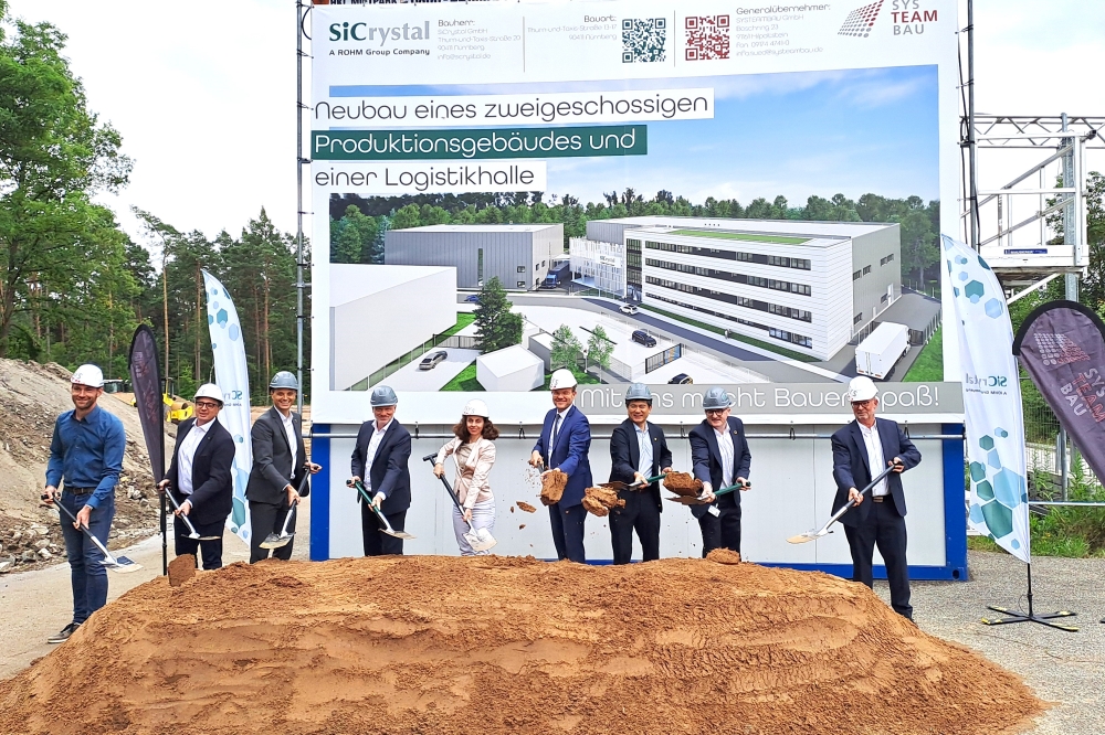
SiCrystal GmbH, a subsidiary of the Japanese Rohm Group, will create additional SiC wafer production production space in the north-east of Nuremberg, directly opposite its existing site.
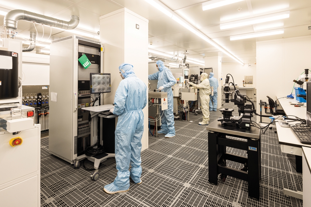
The new building will offer an additional 6,000 m2 of production space and will be equipped with state-of-the-art technology to further optimise the production of SiC wafers, according to the company. The close proximity to the existing plant will ensure close integration of the production processes.
SiCrystal's total production capacity, including the existing building, will be approximately three times higher in 2027 than in 2024.
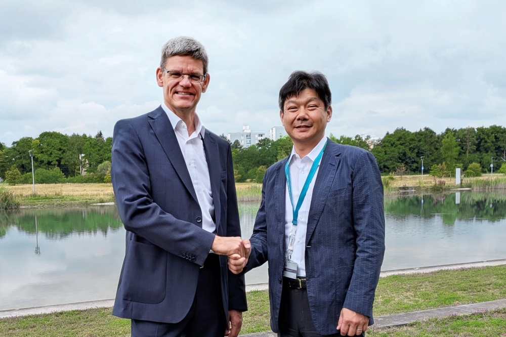
“The new space will significantly increase the production capacity for SiC substrates and we are proud that we were able to welcome Mayor König to the ground-breaking ceremony," says Robert Eckstein, CEO of SiCrystal.
"This groundbreaking ceremony marks an important milestone for SiCrystal and underlines our commitment to the metropolitan region." said Erwin Schmitt, COO of SiCrystal. "With the additional production capacities, we will strengthen our market position and make an important contribution to technological development in the semiconductor industry."
Nuremberg's Mayor Marcus König said: "SiCrystal is one of the world's leading manufacturers of SiCsemiconductor substrates - among other things, these products are needed for the energy transition. I am delighted that SiCrystal is committing itself to Nuremberg as a location with this massive investment and is thus not only retaining jobs but also creating new ones. Nuremberg is an attractive location."
The construction work is scheduled to be completed by the beginning of 2026.


