NCT awarded NEDO gallium oxide project
Novel Crystal Technology (NCT) has been awarded a five year $31M (4.5 billion yen) R&D project to develop β-Ga2O3 wafers, power devices, and power modules by Japan's New Energy and Industrial Technology Development Organisation (NEDO).
NCT will collaborate with Mitsubishi Electric and Japan Fine Ceramics Center.
The 'Development of Material Technology for High-Output and High-Efficiency Power Devices / High-Frequency Devices' project is part of an advanced technology program promoted by the Cabinet Office (CAO), the Ministry of Education, Culture, Sports, Science and Technology (MEXT), and the Ministry of Economy, Trade and Industry (METI) in Japan.
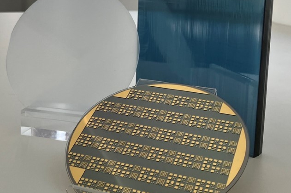
Within the project, NCT will work on the development of low-cost crystal growth technology for manufacturing of 6-inch high-quality β-Ga2O3 wafers and 6-inch homoepitaxial growth technology with low defect density and high production throughput.
In addition, in collaboration with Mitsubishi Electric, it will work on the development of a high-voltage β-Ga2O3 transistor with high breakdown voltage at 3.3 kV or more, and low on-resistance which is less than one-half that of SiC. Mitsubishi Electric will also work on the development of a power module in which multiple β-Ga2O3 transistor chips are assembled in parallel.
Japan Fine Ceramics Center will work on the construction of a non-destructive, high-speed full-surface defect inspection technology for 6-inch β-Ga2O3 wafers.