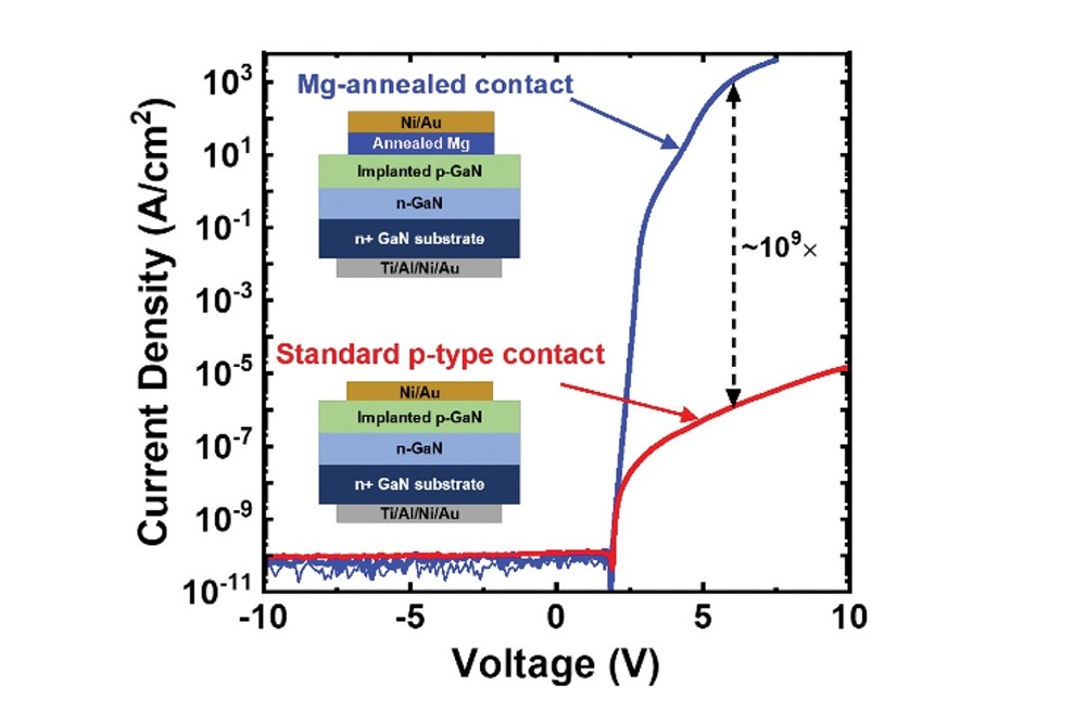
Axus says CMP tool offers lowest cost of ownership
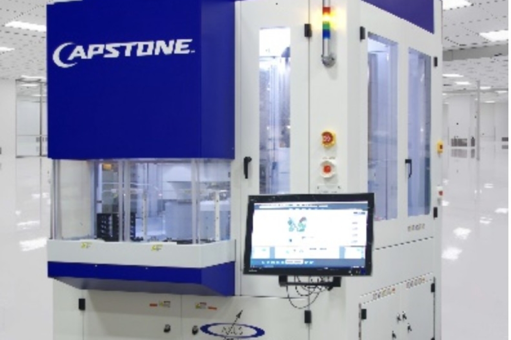
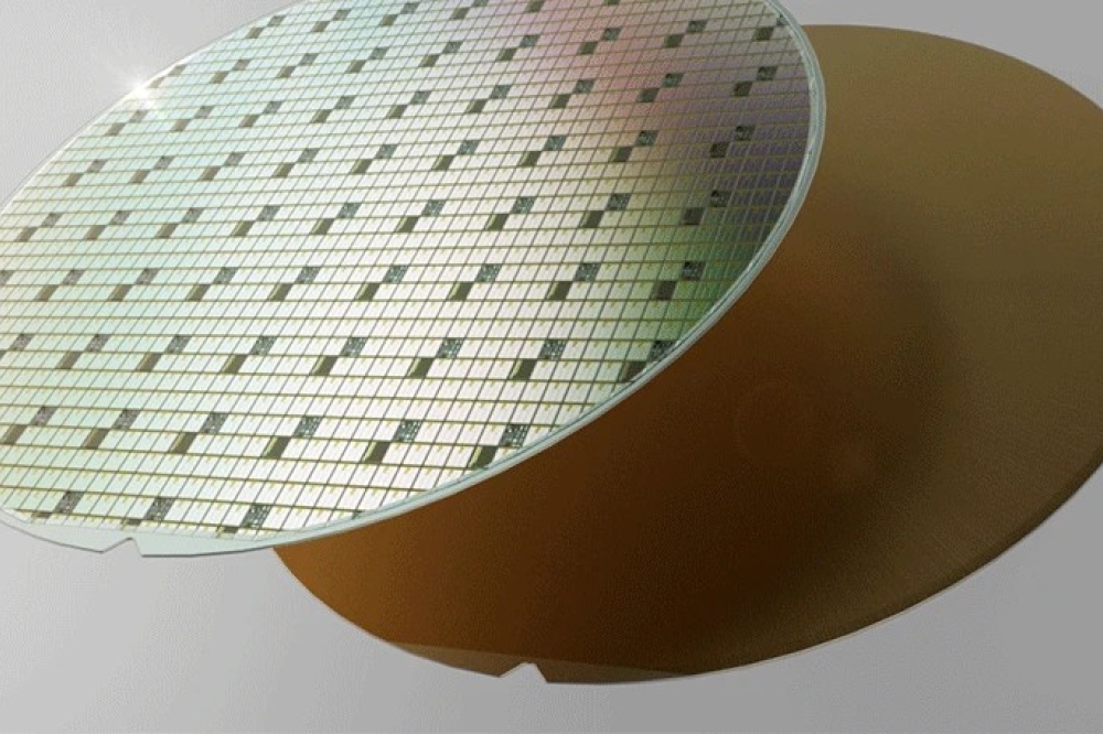
Axus Technology, a provider of chemical mechanical planarisation (CMP) equipment, has announced its Capstone CS200 platform tools offer the industry’s lowest cost of ownership (CoO) for CMP processes on 200mm SiC wafers.
The company says that compared to its closest competitor, the small-footprint Capstone delivers twice the throughput at less than half the total cost per wafer.
“Many 200mm fabs are looking to upgrade their installed base of CMP tools to products with leading-edge capability and functionality. Our ability to deliver industry-low CoO further underscores our strong market position and capacity to support this shift,” said Axus Technology CEO Dan Trojan.
He added: “Capstone features a streamlined workflow and integrated cleaning capability, so it requires half the process steps of older CMP tools. This allows customers to greatly lower their capex investment.”
Figures from the company say that compared to its closest competitor, Capstone offers throughput of 2.5x wafers per hour; 60 percent lower power consumption; 80 percent lower DI water consumption; 45 percent smaller footprint; 65 percent lower capex cost per wafe; and 50 percent lower total cost per wafer.
Another factor contributing to Capstone’s lower CoO is its built-in Process Temperature Control (PTC) technology, which enables processing at higher pressures and speeds without exceeding temperature limits of polishing pads and other sensitive components. This feature is vital for SiC and other materials with high hardness and planarisation challenges that necessitate more aggressive process conditions.
The company says it will be on hand to discuss CMP advantages further at the upcoming International Conference on Silicon Carbide and Related Materials (ICSCRM), Sept. 29-Oct. 4, at the Raleigh, Convention Center, North Carolina, USA.