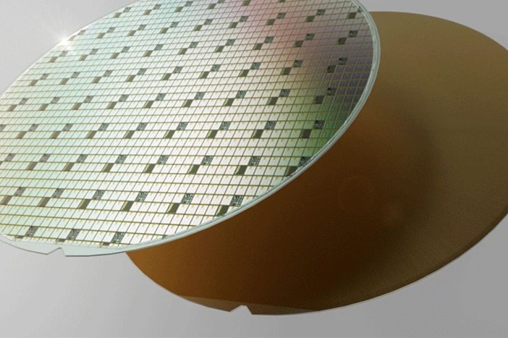
Soitec and Resonac sign SmartSiC agreement

The Japanese company Resonac (formerly Showa Denko) and France-based materials company Soitec have signed an agreement to develop 200mm (8-inch) SmartSiC SiC wafers using Resonac substrates and epitaxy processes, in a major step for the deployment of Soitec’s high-yielding SiC technology in Japan and other international markets.
Christophe Maleville, CTO at Soitec, commented: “SiC is being adopted for EV and industrial applications, where it brings a significant system cost advantage. To further accelerate this adoption, SiC yield and productivity must be improved. Associating Resonac premium quality SiC materials with Soitec’s unique 200mm (8-inch) SmartSiC technology will support volume availability of record quality epi-ready substrate. The combination of our respective technologies and products will optimise these substrates using Resonac’s high-quality epitaxy. Soitec is proud and excited to be partnering with Resonac to develop a best-in-class combined SiC product offering for Japan and the world.”
Makoto Takeda, general manager of device solutions business unit at Resonac, commented: “We are delighted to announce this partnership with Soitec, which is fully aligned with our broader commitment to sustainable and energy-efficient semiconductor solutions. By combining Resonac’s high quality monocrystalline SiC wafers with Soitec’s unique SmartSiC technology, we will deliver improved production efficiency of 200mm (8-inch) SiC wafers and diversify the epi-wafer supply chain.”
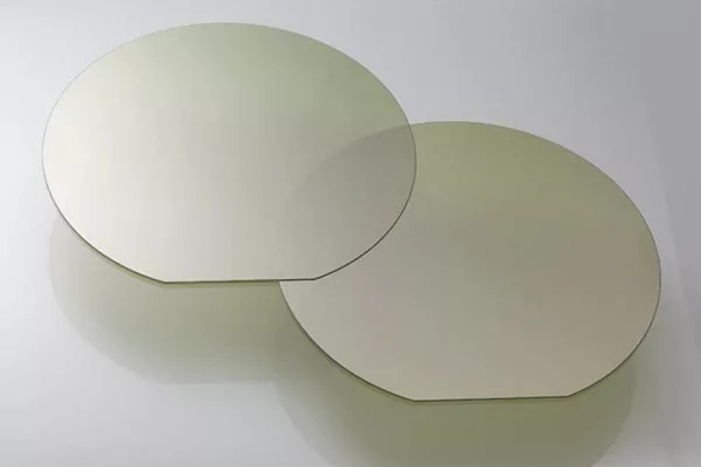
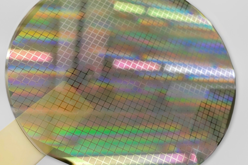
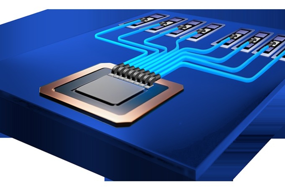
Soitec’s SmartSiC SiC wafers, or engineered substrates, are produced using the company’s proprietary SmartCut technology to bond an ultra-fine layer of high-quality mono-SiC ‘donor’ wafer to a low-resistivity polycrystalline (poly-SiC) ‘handle’ wafer. The resulting engineered substrate is said to delivers significantly improved device performance and manufacturing yields. By allowing multiple re-uses of the prime quality mono-SiC wafer, the process also reduces overall energy consumption during wafer manufacturing.
Soitec has a new fabrication plant at its headquarters in Bernin, France, primarily dedicated to the production of SmartSiC wafers for electric vehicles, renewable energy and industrial equipment component applications.