Speeding up the discovery of materials
Researchers from Tohoku University and the Massachusetts Institute of Technology (MIT) have unveiled a new AI tool for high-quality optical spectra with the same accuracy as quantum simulations, but working a million times faster, potentially accelerating the development of photovoltaic and quantum materials.
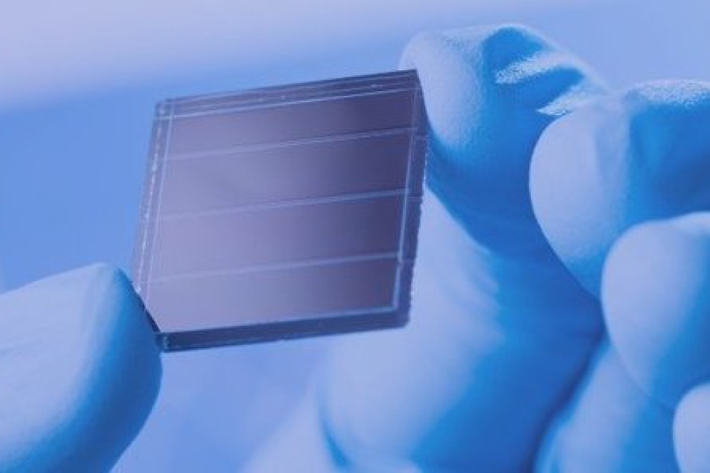
Understanding the optical properties of materials is essential for developing optoelectronic devices, such as LEDs, solar cells, photodetectors, and photonic integrated circuits. These devices are pivotal in the semiconductor industry's current resurgence.
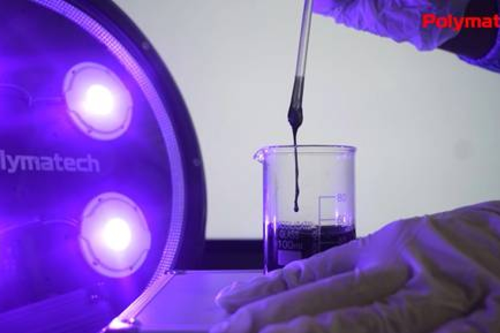
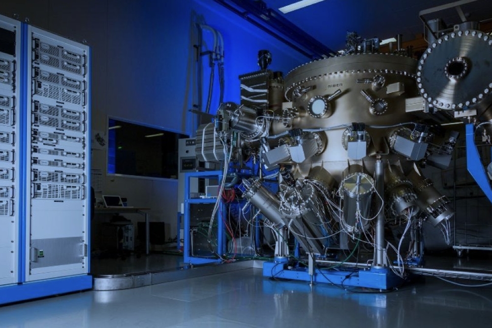
Traditional means of calculation using the basic laws of physics involve complex mathematical calculations and immense computational power, rendering it difficult to quickly test a large number of materials. Overcoming this challenge could lead to the discovery of new photovoltaic materials for energy conversion and a deeper understanding of the fundamental physics of materials through their optical spectra.
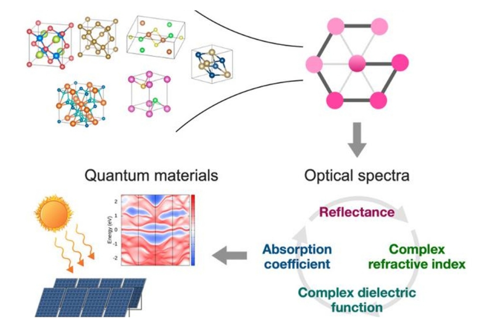
A team led by Nguyen Tuan Hung, an assistant professor at the Frontier Institute for Interdisciplinary Science (FRIS), Tohoku University, and Mingda Li, an associate professor at MIT's Department of Nuclear Science and Engineering (NSE), did just that, introducing a new AI model that predicts optical properties across a wide range of light frequency, using only a material's crystal structure as an input.
Lead author Nguyen and his colleagues recently published their findings in an open-access paper in Advanced Materials.
"Optics is a fascinating aspect of condensed matter physics, governed by the causal relationship known as the Kramers-Krönig (KK) relation," says Nguyen. "Once one optical property is known, all other optical properties can be derived using the KK relation. It is intriguing to observe how AI models can grasp physics concepts through this relation."
Obtaining optical spectra with complete frequency coverage in experiments is challenging due to the limitations of laser wavelengths. Simulations are also complex, requiring high convergence criteria and incurring significant computational costs. As a result, the scientific community has long been searching for more efficient methods to predict the optical spectra of various materials.
"Machine-learning models utilised for optical prediction are called graph neural networks (GNNs)," points out Ryotaro Okabe, a chemistry graduate student at MIT. "GNNs provide a natural representation of molecules and materials by representing atoms as graph nodes and interatomic bonds as graph edges."
Yet, while GNNs have shown promise for predicting material properties, they lack universality, especially in representations of crystal structures. To work around this conundrum, Nguyen and others devised a universal ensemble embedding, whereby multiple models or algorithms are created to unify the data representation.
"This ensemble embedding goes beyond human intuition but is broadly applicable to improve prediction accuracy without affecting neural network structures," explains Abhijatmedhi Chotrattanapituk, an electrical engineering and computer science graduate student at MIT.
The ensemble embedding method is a universal layer that can be seamlessly applied to any neural network model without modifying the neural network structures. "This implies that universal embedding can readily be integrated into any machine learning architecture, potentially making a profound impact on data science," says Mingda Li.
This method enables highly precise optical prediction based solely on crystal structures, making it suitable for a wide variety of applications, such as screening materials for high-performance solar cells and detecting quantum materials.
Looking ahead, the researchers aim to develop new databases for various material properties, such as mechanical and magnetic characteristics, to enhance the AI model's capability to predict material properties based solely on crystal structures.