DARPA awards $3M for heterogenous integration research

The University of Michigan has won $3M funding to develop CMOS-compatible, defect-free universal growth of III-N and III-V multilayer heterostructures on silicon.
This is part of DARPA’s Material Synthesis Technologies for Universal and Diverse Integration Opportunities (M-STUDIO) initiative. The goal of M-STUDIO is to realise a "universal heterogeneous integration technology, compatible with leading edge and future advanced-node semiconductor manufacturing processes, via atomic-precision nano-scale multi-layer material synthesis.”
“We must find new materials that have fundamentally better properties than silicon, as far as transistor functionality, but they need to be integrated into the current manufacturing processes,” explained Zetian Mi, University of Michigan professor of Electrical and Computer Engineering, who is in charge of the project . “It’s not likely for the industry to give up many billions of dollars of infrastructure. As such, the new material should ideally be CMOS compatible.”
Mi’s research group has focused on developing these new materials for many years, growing pristine single-crystalline ferroelectric III-V compounds, such as GaN, in the laboratory at nanoscales. Mi knows that these materials must be scalable and compatible with silicon to transition into devices, and his newest grant support from the Defense Advanced Research Projects Agency (DARPA) will bring his team closer to this goal
For the new DARPA project, Mi and his collaborators, Kai Sun (U-M Materials Science and Engineering) and Patrick Fay (University of Notre Dame), will use a new method to grow ultra-thin layers of III-V compound crystals without a foreign metal catalyst, which often introduces impurities. These tens-of-atoms thick layers will allow Mi’s team to grow the semiconductor materials on silicon lattice without defects. The final goal of this project will be to partner with the manufacturing company Intelligent Epitaxy Technology, Inc (IntelliEPI) to show viability of this material at scale for use in industry.
“We are looking into the fundamental, long-standing challenge of integrating compound semiconductors with silicon,” said Mi. “It’s a very difficult problem, but if we are successful, there is the possibility that this material will go into every computer, every cell phone, virtually every electronic device that we use.”
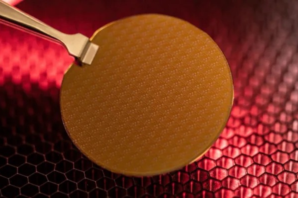
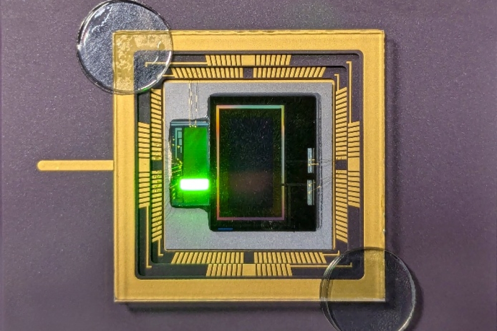
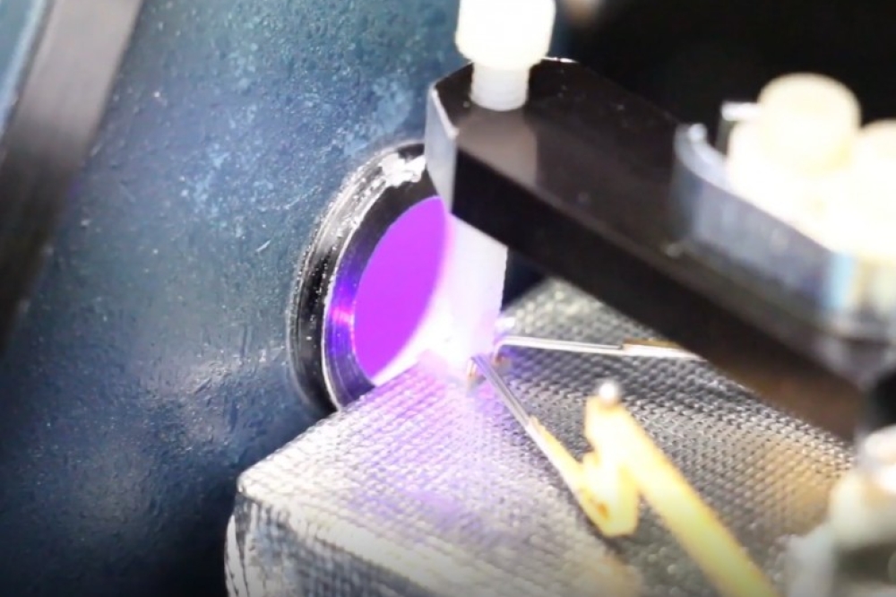
Pictured above: A sample of monolayer III-nitrides on a foreign substrate, an example of a III-V semiconductor material, previously grown by MBE in Zetian Mi’s laboratory. Photo: Brenda Ahern, Michigan Engineering

