Loading...
News Article

NexGen Wafer Systems introduces new platform

News
Sereno multi-chamber wet etch and clean platform features integrated metrology for 6inch, 8 inch, and 12 inch substrates

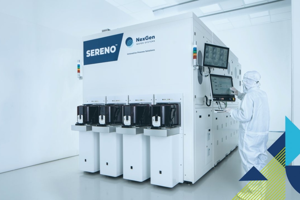
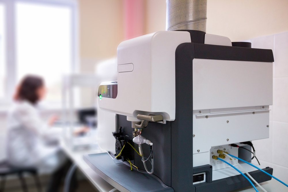
NexGen Wafer Systems has launched Sereno, its latest multi-chamber platform designed for Wet Etch and Clean applications. It supports 6inch, 8 inch, and 12 inch substrates made from Silicon, SiC, GaN, GaAs, Al2O3 and ZnO.

Sereno is said to combine high performance with flexibility, offering integrated metrology for precise substrate and layer thickness control, as well as surface roughness control. Its onboard chemical supply system supports multiple process chemicals with integrated mixing, blending, and comprehensive analytics, ensuring maximum adaptability across a wide range of applications.

It has a footprint of less than 12 m² and a throughput of up to 200 wafers per hour. It can support wafer thicknesses ranging from ultra-thin wafers below 100µm to bonded wafers exceeding 2mm in total thickness.

“With Sereno, we provide Wet Etch and Clean solutions that deliver high throughput in a compact footprint while maximising the flexibility and performance advantages of Single-Wafer Technology,” said Christian Kleindienst, chief marketing officer at NexGen Wafer Systems. “Our Sereno platform addresses our customers' demand for flexible, high-performance Single-Wafer solutions that reduce operational costs and present a highly attractive alternative to traditional batch tools.”

The Sereno platform is now available for orders, with first deliveries starting in Q1 2025.

SPONSOR MESSAGE

Secure Your Hydrogen Supply

A study supply of high-purity hydrogen is critical to semiconductor fabrication. Supply chain interruptions are challenging manufacturers, leading to production slowdowns and stoppages. On-site hydrogen generation offers a scalable alternative for new and existing fabs, freeing the operator from dependence on delivered gas.

Plant managers understand the critical role that hydrogen plays in semiconductor fabrication. That important job includes crystal growth, carrier gas, wafer annealing, and in the emerging Extreme UV Lithography (EUV) that will enable new generations of devices. As the vast need for semiconductors grows across all sectors of world economies, so does the need for high-purity hydrogen.

Take control with Nel on-site hydrogen generation.

Read more
×
Search the news archive

To close this popup you can press escape or click the close icon.
Logo
x
Logo
×
Register - Step 1

You may choose to subscribe to the Compound Semiconductor Magazine, the Compound Semiconductor Newsletter, or both. You may also request additional information if required, before submitting your application.


Please subscribe me to:


You chose the industry type of "Other"

Please enter the industry that you work in:
 
x
Adblocker Detected
Please consider unblocking adverts on this website