Toshiba samples latest 1200V SiC MOSFETs
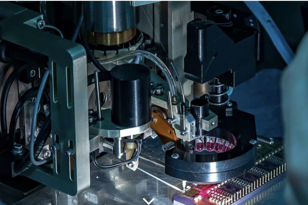
Toshiba Electronics Europe has announced early test samples in bare die format of new 1200V SiC MOSFETs with low on-resistance (RDS(ON)) and high levels of reliability. The devices are suited to applications within automotive traction inverters.
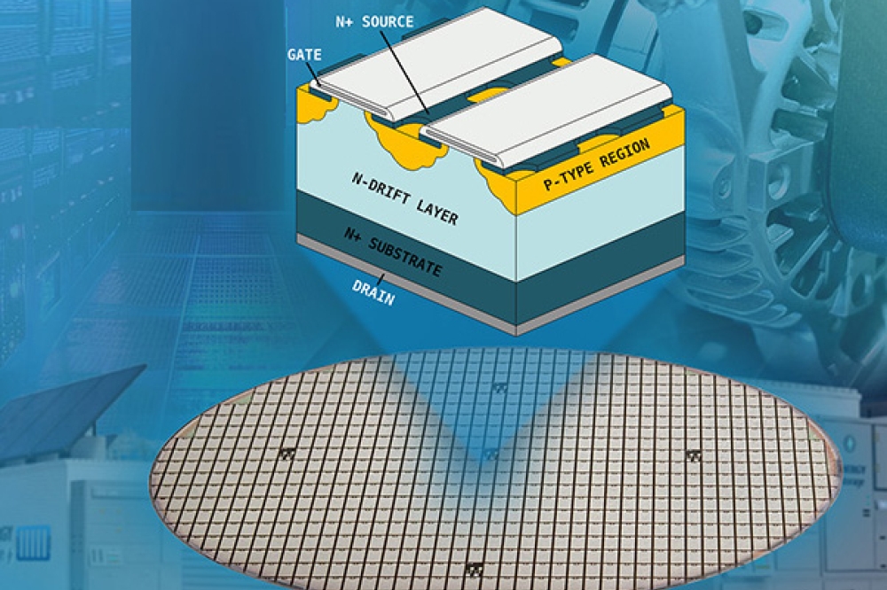
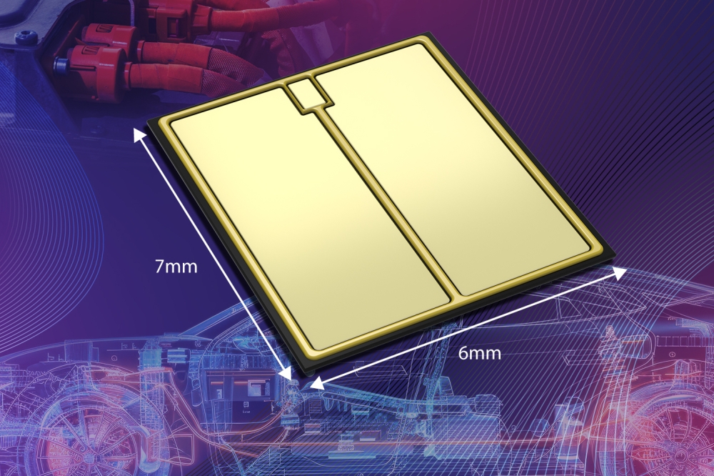
The new X5M007E120 uses a manufacturing process that reduces on-resistance per unit area by up to 30 percent, according to the company. Unlike existing methods that utilise a striped-pattern construction, the new devices arrange the embedded Schottky barrier diodes (SBDs) in a check-pattern to achieve lower on-resistance.
Many SiC MOSFETs increase on-resistance as body diodes are energised during reverse conduction, which can lead to reliability issues. Toshiba SiC MOSFETs alleviate this issue by preventing body diodes from operating as SBDs are embedded into the MOSFETs. This approach maintains the reduction in on-resistance while ensuring reliability during reverse conduction.
The re-arrangement of SBDs in this device has suppressed body diode energisation, and the upper limit of unipolar operation has increased to around double without increasing the SBD mounting area. Additionally, channel density is improved. These enhancements contribute to energy efficiency in applications, including motor control inverters.
Reducing RDS(ON) within a SiC MOSFET can cause excess current flow during short-circuit operations. By adopting a deep barrier structure, the X5M007E120 reduces excessive current within the MOSFET section and leakage current in the SBDs section during short-circuit operation. This enables durability during short-circuit conditions while maintaining high levels of reliability against reverse conduction operation.
The new X5M007E120 has a VDSS of 1200V and is rated for a drain current (ID) of 229A continuously, with 458A for pulsed operation (ID Pulse). RDS(ON) is as low as 7.2mΩ, and the device can operate with channel temperatures (Tch) as high as 175°C. The devices are AEC-Q100 qualified for automotive applications.
Engineering samples of the new X5M007E120 are expected to ship during 2025, with mass production samples scheduled to start in 2026.