Loading...
News Article

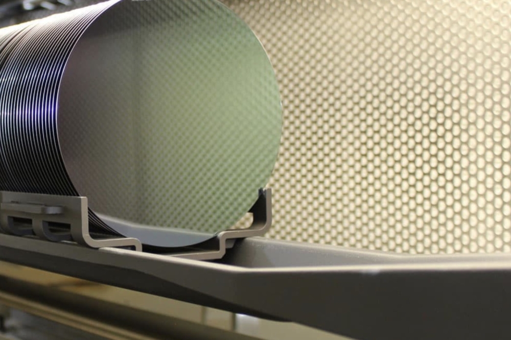
US DOE announces $481.5m loan to SK Siltron CCS

News
Company to use funds to expand manufacturing of SiC wafers for EVs

As part of the Biden-Harris Administration’s Investing in America agenda, the Department of Energy (DOE) has announced a $544 million loan to SK Siltron CCS, LLC to expand American manufacturing of high-quality SiC wafers for electric vehicle (EV) power electronics.

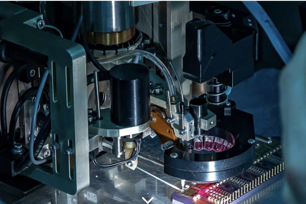
The project — located at SK Siltron CSS facility in Bay City, Michigan — is expected to be among the top-five manufacturers of SiC wafers globally, boosting America’s manufacturing competitiveness.

This project is forecast to create up to 200 construction jobs in the build-out phase and up to 200 skilled, good-paying operations jobs at full production.

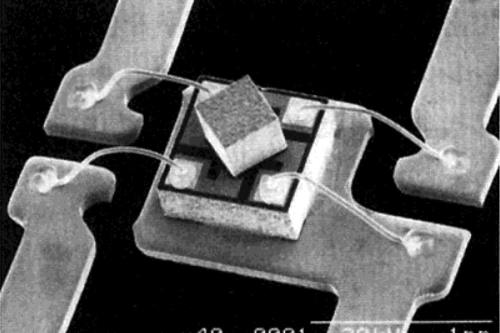
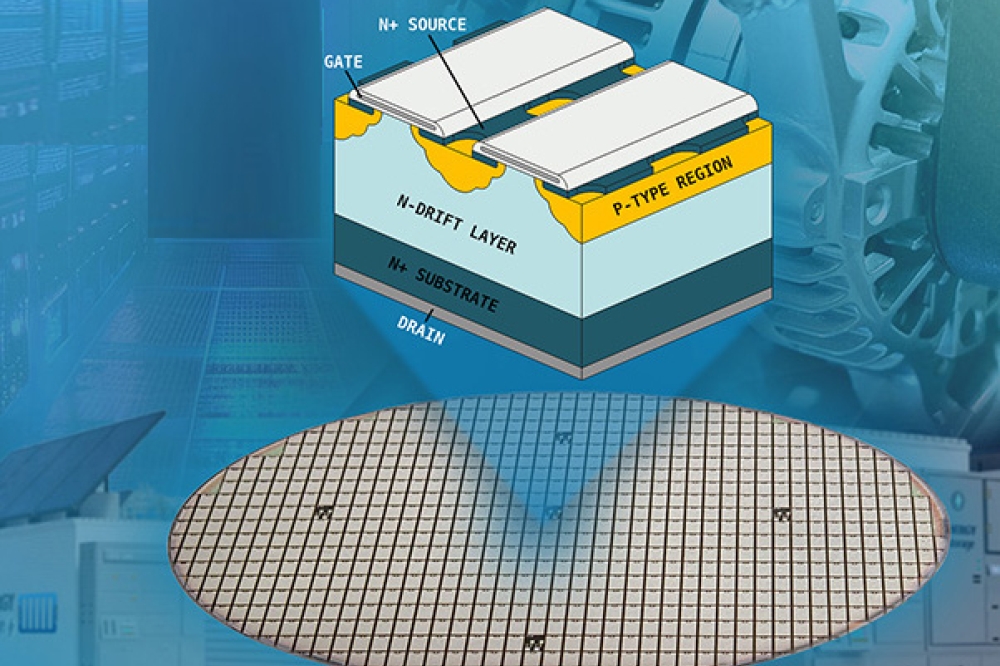
SK Siltron CSS sells directly to device manufacturers which make power electronics used across many industries, not just EVs and high-speed EV charging. Market demand is currently being driven by transportation, next generation cellular (i.e., 5G), artificial intelligence and cloud computing end uses. SiC is also becoming increasingly common in other mid to high voltage applications such as solar photovoltaic, inverters and DC converters, and industrial chargers and adapters.

The loan is offered through LPO’s Advanced Technology Vehicles Manufacturing (ATVM) Loan Program, which supports domestic manufacturing of advanced technology vehicles, qualifying components, and materials that improve fuel economy.

SPONSOR MESSAGE

Secure Your Hydrogen Supply

A study supply of high-purity hydrogen is critical to semiconductor fabrication. Supply chain interruptions are challenging manufacturers, leading to production slowdowns and stoppages. On-site hydrogen generation offers a scalable alternative for new and existing fabs, freeing the operator from dependence on delivered gas.

Plant managers understand the critical role that hydrogen plays in semiconductor fabrication. That important job includes crystal growth, carrier gas, wafer annealing, and in the emerging Extreme UV Lithography (EUV) that will enable new generations of devices. As the vast need for semiconductors grows across all sectors of world economies, so does the need for high-purity hydrogen.

Take control with Nel on-site hydrogen generation.

Read more
×
Search the news archive

To close this popup you can press escape or click the close icon.
Logo
x
Logo
×
Register - Step 1

You may choose to subscribe to the Compound Semiconductor Magazine, the Compound Semiconductor Newsletter, or both. You may also request additional information if required, before submitting your application.


Please subscribe me to:


You chose the industry type of "Other"

Please enter the industry that you work in:
 
x
Adblocker Detected
Please consider unblocking adverts on this website