
Laminates improve perovskite PV performance
A collaborative research team from the Hong Kong University of Science and Technology (HKUST) and the Hong Kong Polytechnic University (PolyU) has developed an innovative laminated interface microstructure that enhances the stability and photoelectric conversion efficiency of inverted perovskite solar cells.
The team’s research findings have been published in Nature Synthesis, in a paper titled 'Synthesis of a Lattice-Resolved Laminate-Structured Perovskite Heterointerface'.
The basic structures of perovskite solar cells are classified into two types: standard and inverted. The inverted structure demonstrates better application prospects because the electronic materials used in each layer are more stable compared to those in the standard configuration.
However, challenges related to interface science still exist in inverted devices, particularly concerning defect accumulation at the interface between the fullerene-based electron transport layer and the perovskite surface. This defect accumulation significantly impacts the device’s performance and stability.
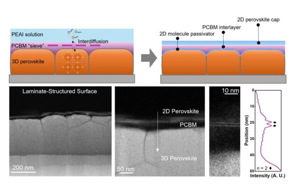
Zhou Yuanyuan, associate professor in the department of chemical and biological engineering (CBE) and associate director of the Energy Institute at HKUST and Cai Songhua’s team from the department of Applied Physics at PolyU have shown that uniformly creating a 'molecular passivation layer-fullerene derivative layer-2D perovskite layer' — a three-ply laminated structure on the surface of the perovskite film — they could effectively reduce the density of interface defects and improve energy level alignment.
This advancement substantially boosts the photoelectric conversion efficiency of the perovskite solar cell and enhances the durability of the interface under damp-heat and light soaking conditions.
They report conversion efficiencies up to 25.97 percent, together with enhanced device stabilities under protocols standardised by the International Summit on Organic Photovoltaic Stability, showing T90 lifetimes (the time at which they maintain 90 percent of their efficiency) of over 1,000 h in both the damp-heat test (85 °C, 85 percent relative humidity) and maximum power point tracking under one-sun illumination.
Guo Pengfei, co-first author of this work and a postdoctoral fellow at HKUST’s CBE Department, said, “We introduced the concept of composite materials into the interface design of optoelectronic devices, allowing the synergistic effects of each layer in this new interface to achieve results that are unattainable with traditional interface engineering.”
Yuanyuan, the lead corresponding author of the study, added, “Perovskite is a soft lattice material. We can create microstructural features in this type of material that are difficult to achieve with conventional materials. Our aim is to understand the formation and mechanisms of these microstructures at the nanoscale, or even at the atomic scale, to drive device innovation based on this fundamental understanding.”
Pictured above: Schematic diagram of the synthesis method of laminated-structured perovskite interface and its structure revealed by transmission electron microscopy.


