

Unifying III-Vs and silicon with an RF interposer
Compact heterogeneous systems are set to benefit from a RF silicon interposer platform that delivers low-loss, high-density interconnects up to 325 GHz.
BY XIAO SUN FROM IMEC
Extraordinary things happen when you bring together the worlds of silicon and compound semiconductors. It’s a marriage that benefits from the scale, manufacturability and integration density of silicon, traits demanded by modern digital systems. And it’s a pairing that draws on the strengths of III-Vs, such as InP and GaN, that provide high power, gain, and speed that’s essential for millimetre-wave and sub-terahertz front-ends. For decades, these two domains have evolved in parallel, separated by fundamental differences in materials, processing, and cost. But the times, they are a changing.
Helping to bridge the gap is a new RF silicon interposer platform developed by our team at imec. This purpose-built technology is capable of uniting these two disparate worlds, by providing a common substrate that allows InP power amplifiers, SiGe LNAs, and CMOS control logic to coexist, interact, and thrive.

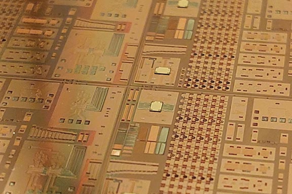
Figure 1. An RF silicon interposer for next-generation high-performance RF and mixed-signal applications.
Designed for chiplet-based heterogeneous systems, our platform provides a record-low loss and an exceptionally broadband performance from 20 GHz to beyond 300 GHz. This breakthrough opens the door to next-generation extreme data-rate short-range radio, high-resolution radar, terahertz imaging, and high-speed wireline systems.
Why heterogeneous integration matters
As communication systems move up in frequency to the D-, G-, and J-bands – that’s 110 GHz to 170 GHz, 140 GHz to 220 GHz, and 220 GHz to 325 GHz – there are increasingly pronounced trade-offs between speed, power, and integration. There is much to like concerning compound semiconductors, such as InP and GaN, as they continue to deliver superior performance for high-power, high-frequency applications – but they remain expensive, are difficult to scale, and they lack the mature backend infrastructure silicon provides. Due to this state-of-affairs, the future of millimetre-wave and sub-terahertz electronics is not about selecting silicon or III-V technologies – it’s about integrating them intelligently.
Guided by this philosophy, we have developed a 300 mm RF silicon interposer (see Figure 1) that brings together low-loss, polymer-based RF routing and fine-pitch digital interconnects. With our interposer, one can bridge analogue and digital domains within a single, scalable platform. Our technology features a new portfolio of compact, low-loss, high-Q passive components, alongside thermally managed chiplet assemblies that fully leverage the strengths of each semiconductor technology.

Figure 2. An RF silicon interposer demonstrator consists of a standard,
low-resistivity silicon substrate, a full ground shield, three
spin-coated low RF loss polymer layers (POLY1, POLY2, POLY3), three
thick metal layers (RDL1, RDL2, UBM) and micro-bumps.
Our journey toward heterogeneous RF integration began with our first-generation silicon interposer, introduced in 2022 and characterised up to 110 GHz. That platform used a moderately resistive silicon substrate (15-25 Ω cm), shielded by a 1 µm copper ground plane, to reduce substrate losses.
This first-generation interposer featured a pair of stacked BCB dielectric layers, implemented to minimise parasitic capacitance and conductor losses. By leveraging BCB’s low dielectric loss and stable permittivity, we realised a high-fidelity millimetre-wave interconnect. However, as applications pushed beyond 140 GHz and required additional routing layers, we hit a wall, impaired by the processing limitations of BCB.
To address this issue, we have developed a second-generation platform, replacing BCB with CYCLOTEN XP80 – it’s a photo-imageable, low-loss RF polymer, produced by DuPont and now sold through its spin-off, Qnity Electronics. XP80 is a great polymer, retaining the excellent dielectric properties of BCB while offering better mechanical stability, reduced internal stress and improved processability – qualities that enable the stacking of multiple redistribution layers (RDLs) for higher-density routing. Note that this material is not a ‘forever chemical’, aligning with the industry’s shift toward environmentally safer materials.
Inside the RF Interposer
Our latest 300 mm silicon-based RF interposer integrates three thick copper RDLs with three polymer layers to form a multilayer stack capable of routing both RF and digital signals with minimal loss. The layer composition, illustrated in Figure 2, has: a MET1DAM ground plane, which serves as an RF shield, minimising substrate-induced losses in silicon; 15 µm-high copper pillars, which provide vertical connections between the BEOL ground plane and the upper interconnect layers; three XP80 polymer layers (thicknesses 15 µm, 7 µm, and 7 µm), which offer electrical isolation and act as low-loss RF waveguides; copper RDL1 and RDL2 (3 µm-thick each), dedicated to low-loss RF signal routing; a 5 µm-thick ‘under-bump utilisation’ layer, which supports bump interconnects for die-to-interposer connections; and CuNiSn micro-bumps, enabling thermocompression bonding of InP, GaN, or CMOS dies.
By supporting routing pitches of 5/5 µm for RF lines, and 1/1 µm for digital interconnects, this advanced stack delivers the integration density and performance required for next-generation mixed-signal and heterogeneous systems.
The greatest triumph of our interposer is its ultra-low transmission loss, a critical metric for millimetre-wave packaging. According to our characterisation of microstrip lines of 1-3 mm, based on frequencies from 20 GHz to 325 GHz and using thru-reflect-line calibration, at 140 GHz insertion losses are 0.30 dB mm-1 and 0.23 dB mm-1 for RDL1 and RDL2, respectively, and the corresponding reflections are below -19 dB and -22 dB. At the higher frequencies of 220 GHz and 325 GHz, losses remain below 0.6 dB mm-1 and 0.9 dB mm-1, respectively.

Figure 3. Insertion loss for 1 mm, 2 mm, and 3 mm long microstrip lines on RDL2.
To put these figures in perspective, note that they are comparable to or better than those for advanced glass interposers and PCBs (see Figure 3). The lower losses are much valued, as they translate directly into a higher amplifier efficiency and better signal integrity, essential for compound semiconductor modules. By combining smooth copper surfaces with the XP80’s low loss tangent, stable performance is possible, even up to the J-band, a milestone for sub-terahertz packaging.
It is essential to have precise knowledge of XP80’s dielectric properties when co-designing interconnects, antennas, and high-Q passives. We have equipped ourselves with this information by using patch-antenna and resonator-based methods to extract the dielectric constant and loss tangent up to 325 GHz (see Figure 4).
For this work we used microstrip patch antennas, designed for 110 GHz, 140 GHz, 170 GHz, 250 GHz, and 300 GHz. The measured results, closely matching simulations, provide values of 2.6 for the relative permittivity and 0.009 for the dielectric loss tangent. After tuning simulations to match our measurements, we derived an average relative permittivity of 2.55, with a variation across the full frequency range of just ± 1.5 percent. After confirming these values with resonator structures, including ring and gap-coupled types, we concluded that we had produced broadband impedance-controlled interconnects.

Figure 4. Comparison between measured and simulated reflection coefficients using an adjusted substrate permittivity of 2.55.
Thermal management
Outstanding electrical performance counts for little, unless it’s accompanied by effective thermal control. In high-power modules, InP and GaN amplifiers may generate intense heat – as high as several watts per millimetre of gate width – making thermal management a defining factor for reliability and lifetime.
To tackle this challenge, we have built thermal intelligence directly into our RF silicon interposer. This is realised through seamlessly embedding microscale heaters and sensors within the RDL and back-end-of-line layers, where copper meanders – just 200 µm by 200 µm in RDL1 and 100 µm by 100 µm in MET1 – act as both heat sources and precise temperature monitors.
By combining on-chip measurements with advanced finite-element modelling, we have determined a thermal conductivity for the XP80 polymer of around 0.15 W m-1 K-1. This insight, key to accurate thermal prediction and co-design, ensures that even high-power III-V die operate safely and efficiently, thanks to effective thermal-mitigation strategies.

Figure 5. Top view of an InP chiplet mounted on the RF silicon interposer showing RF input/output and DC probes.
In short, we have a proven platform that ensures RF performance and thermal reliability go hand-in-hand – supporting the next-generation of compact, high-power, and thermally balanced millimetre-wave and sub-terahertz systems.
As the ultimate proof of this concept, we have co-packaged a two-stage differential InP power amplifier – designed using Teledyne’s 250 nm InP HBT process – directly onto our RF silicon interposer (see Figure 5). Fabrication involved flip-chip bonding of the die via CuNiSn micro-bumps, with the entire assembly process kept below 250 °C to protect delicate InP back-end metallisation.
Measurements of post-assembly performance confirm that our interposer introduces no measurable degradation (see Figure 6). This effort has determined a small-signal gain of 16.3 dB, a 3 dB bandwidth that spans 116 GHz to 148 GHz, an input/output match that’s better than -10 dB, and a reverse isolation of -40 dB.
When driving this co-packaged system under large-signal operation at 130 GHz, we recorded a value for P1dB – that’s the input or output power level where the device’s gain drops by 1 dB from its ideal linear gain – of 13-15 dBm. Power-added efficiency (PAE) is between 15 percent and 28 percent (see Figure 7), closely matching the performance of standalone InP power amplifiers.
The key point to be taken from these results is that our silicon interposer technology introduces virtually no parasitic penalty, validating the precision of our design and fabrication processes. Our success is a major step towards fully co-packaged III-V and silicon systems, where high power meets high integration on a single scalable platform.

Figure 6. Solid lines represent the small signal S-parameters of the PA
at reference plane P1. By subtracting the loss of the rat-race hybrid
(black line) from the S21 of the PA between P1-P1 (solid magenta), the
reference plane can be shifted to the S21 of the PA between P2-P2
(dashed magenta).
Serving compound semiconductor systems
There has been little change in the semiconductor status quo over the last few years. Silicon continues to dominate logic and memory, while compound semiconductors, such as InP and GaN, excel in RF and photonic performance.
Our RF silicon interposer brings these strengths together, providing a CMOS-compatible, 300 mm manufacturable substrate for scalable integration of compound chiplets. With this approach, as well as enabling high-density routing, our platform offers a thermal advantage, with silicon providing a superior thermal conductivity to glass and PCB, enabling better heat dissipation. Another merit of our technology is that it’s fully compatible with 300 mm wafer processing in standard CMOS fabs, ensuring manufacturability at scale.
With our architecture, InP and GaN chiplets may be minimised to their active PA cores, while biasing, filtering, and impedance matching are migrated to the interposer. The upshot is a truly heterogeneous system with smaller footprints, lower cost, and higher yield, combining the high performance of III-V devices with the scalability and integration density of silicon.

Figure 7. Large signal parameters of the PA at 130 GHz between reference planes P2-P2.
As our interposer supports multi-band modules, operating from 20 GHz to 325 GHz and thus covering the D-, G-, and J-bands, it is ideal for future high-capacity wireless links, radar, and sensing systems. Its combination of sub-terahertz signal integrity, low-loss routing, thermal co-design, and dense chiplet integration sets a blueprint for next-generation heterogeneous architectures.
In short, our second-generation RF silicon interposer bridges the divide between silicon and compound semiconductors. Particularly noteworthy is XP80 polymer-based RF routing, a low-loss performance up to 325 GHz, and a built-in thermal co-design for reliable high-power operation. These assets have helped us to successfully co-package a fully functional InP D-band amplifier without performance degradation, and to ultimately demonstrates the feasibility of heterogeneous systems, where InP, GaN, SiGe, and CMOS operate side by side.
As the world advances toward next-generation wireless and wireline communications, sub-terahertz sensing, and ultra-fast radar, our interposer stands as more than a packaging solution – it’s the bridge between the precision of silicon and the power of III-Vs.
This work was carried out by the imec teams, with support from Qnity Electronics for the XP80 polymer materials. The author thanks imec colleagues involved in RF interposer design, fabrication, assembly, dielectric characterisation, and thermal modelling for their valuable contributions – Siddhartha Sinha, Martijn Huynen, Reinier Broucke, Melina Lofrano, Vladimir Cherman, Angel Uruena, Ehsan Shafahian, Damien Leech, Nazia Fathima, Andy Miller and Eric Beyne – as well as Nadine Collaert and Joris Van Driessche for their support through the ARF programme.


