

Stress-tested, future-ready GaN
Reliable GaN unlocks the door to a hyper-efficient future where AI thrives, humanoids awaken, and data centres pulse cooler, faster, and smarter.
BY GABRIEL LANSBERGEN AND SAMEH KHALIL FROM INFINEON TECHNOLOGIES
For decades, silicon-based semiconductors have been the bedrock of power electronics. Their deployment has spanned consumer devices, industrial automation and automotives, with devices delivering remarkable scalability and cost efficiency.
But evolution is underway. As global energy demands surge and applications grow more electrified, driven by desire for ‘digitalisation’ and ‘decarbonisation’, wide bandgap devices are making an impression in the power landscape. The era of co-existence is underway, with these three material systems are forming a complementary toolkit: silicon is retaining its dominance in low-to-mid-voltage applications; SiC is now excelling in high-voltage environments, such as grid infrastructure, automotive and industrial applications; and GaN is rapidly gaining ground in high-frequency, high-efficiency domains, such as fast chargers, solar microinverters, radar systems and AI-centric data centres.
In the future, megatrends like e-mobility, AI-driven data factories and humanoid robotics will rely on advanced power electronics to deliver reliable, compact and thermally resilient energy. By 2030, it’s possible that electrified transport and data centres alone will be trimming their energy consumption from what it could have been by over 150 million tons of CO2 every year, thanks to wide bandgap adoption. At the same time, this trend will unlock billions in economic activity across automation, cloud infrastructure and intelligent machines.

Figure 1. Cross-section of the unit cell of Infineon’s high-voltage lateral GaN HEMT, depicting the 2DEG sheet of electron charges and the absence of a p-n junction in the drift region. The higher the off-state breakdown requirements, the longer the gate-to-drain spacing. The high critical-electrical-field makes this distance much shorter than that of silicon counterparts while the high mobility and the high density 2DEG sheet of electron charges provides the low ohmic resistivity.
The attraction of lateral GaN HEMTs
Advantages of GaN-based power devices can be broadly grouped into two categories. First, there’s their intrinsic material properties, including a wide bandgap of 3.44 eV at 300 K, and a high saturation electron drift velocity of 2.5 x 107 cm s-1. And the second strength is their distinct device design, particularly when implemented in a lateral HEMT (see Figure 1) – this architecture allows for an exceptionally low on-state resistance for a given breakdown voltage, enabling enhanced efficiency and a higher power density.
There are also merits that arise from a wider bandgap (see Figure 2). Compared with that for silicon, just 1.12 eV, that for GaN is almost three times higher, ensuring a higher critical electric field that allows device designers to implement more compact unit cells for the same breakdown requirements. A smaller chip area is a major offsetting factor in what otherwise could lead to uncompetitive chip costs. What’s more, the wider bandgap of GaN allows devices made from this material to operate at much higher temperatures, due to a lower intrinsic concentration of the thermally-generated electron-holes pairs, which are a potential source of noise that could hamper optimal device operation, especially under stringent applications conditions.

Figure 2. Comparison between silicon, SiC and GaN at a material level, a device level and a system level, highlighting their unique advantages and complimentary nature.
GaN HEMTs are renowned for their very low specific on-state resistance, a characteristic defined as the product of the on-state resistance and the device area. Contributing to this is a two-dimensional electron charge density reaching up to 1-2 x 1013 cm-2, and an electron mobility as high as 2,000 cm2 V-1 s-1, resulting from GaN’s high saturation electron drift velocity and its ability to form a two-dimensional electron gas layer.
Yet another advantage of the GaN HEMT is its capability to operate at high frequencies, thanks to a lack of minority carriers and a high saturation velocity. Behind this is an absence of a p-n junction diode to hold off an applied voltage in the off-state. The upshot is that circuit designers and system architects can produce smaller, lighter products that handle higher powers using higher frequencies.
Reliability: a mission-critical enabler
As our society accelerates into a future that’s powered by intelligent machines, data factories, electrified mobility and resilient infrastructure, GaN reliability is no longer a checkbox – instead it’s the anchor point of progress, the silent guarantor of robust, high-efficiency power electronics that will shape a world worth living in.
Over the past two decades, engineers, physicists and reliability specialists studying GaN HEMTs have amassed a substantial body of data, driving significant advances in device reliability. These investigations have provided the foundation for product qualifications that meet the stringent demands of consumer, industrial and automotive-grade applications.
At Infineon, we have been playing our part in these efforts, with several key challenges shaping the focus of our work. First, while the critical electric field of GaN – approximately ten times higher than that of silicon – provides the advantage of compact device geometries, as well as the means to operate under much stronger electric fields, particularly at or near the surface, we know that this comes at a price. It places significant stress on passivation and interfacial layers.

Figure 3. Bathtub Curve. Device failures falls under three regimes, long conceptualised by insurance companies in the late 19th and early 20th
centuries to describe mortality rates: a diminishing Early Life Failure
Rates (ELFR), random (constant) failure rate and an increasing
‘wear-out’ failure rates, corresponding to infant mortality, stable
middle years and increased risk of mortality with aging mortality in
humans, respectively.
Our other area of concern relates to heteroepitaxial growth. Most GaN technologies rely on GaN layers, or related III-nitride stacks, that are grown on non-native substrates, predominantly silicon or sapphire. This approach tends to introduce defects and mechanical stress, originating from lattice and thermal mismatches between epitaxial layers and the underlying substrates.
To address these challenges, there needs to be sustained progress in defect reduction, alongside failure root-cause identification, advanced screening methodologies and the gaining of a deeper understanding in the underlying physics driving device degradation mechanisms – all have been central priorities throughout the development phase of our GaN technology.

Figure 4. The comprehensive reliability of GaN-based devices go far beyond baseline JEDEC standards.
Device failures fall under three categories, analogous to and originally conceptualised by insurance companies in the late 19th and early 20th centuries, to describe mortality rates (see Figure 4). These categories, which correspond to humanity’s infant mortality, stable middle years and increased risk of mortality with aging, are: a diminishing early life failure rate; a random (constant) failure rate, and an increasing wear-out failure rate. When considered together, they produce what’s commonly described as a ‘bathtub’ curve, a term coined in the 1950s by aerospace and electronics engineers.
Rigorous methodology
We employ a comprehensive approach to reliability, ensuring that our GaN products meet both the intrinsic (wear out) and the extrinsic (ELFR) failure rates in the field. We use standard JEDEC (Joint Electron Device Engineering Council) tests as a baseline, and turn to rigorous technology and product-accelerated lifetime tests to assess the ELFR and wear-out mechanisms, to estimate failure rates that are tailored to customer-use conditions (see Figure 5).

Figure 5. Qualification methodology depicting the main four inputs that drive product release at Infineon Technologies.
To make sure that we meet reliability and quality criteria, we apply four inputs to the qualification plan. This approach includes the development of statistically viable failure models, which support our efforts to ensure that we meet the system target operating lifetime.
The qualification of our products begins with capturing the Application Profile, which quantitatively describes the stress conditions faced by the device through its lifetime in the application. We also specify the Quality Requirements Profile (QRP), which states quality targets, such as lifetime and Failure-in-Time (FIT) rates targets. During the technology development phase, we uncover device failure modes and mechanisms for both intrinsic and extrinsic failures, and we identify and pursue a path for extrinsic failures reduction. Efforts also include accelerated reliability testing, undertaken to generate degradation models and estimate lifetime and failure rates at use conditions.
Based on these four pillars, we determine a qualification plan that exceeds the standard JEDEC baseline.
To bring the reliability of GaN electronics to new levels, it’s not possible to simply draw on standard techniques established in older material systems. Instead, to break new ground we investigate the reliability of our devices using advanced methodologies that are specifically tailored to the peculiarities of GaN.
One characteristic that’s specific to GaN is its propensity for charge trapping in the buffer layers and the first layer of the passivation, as per Figure 1. Another trait is that due to its polar nature, GaN material suffers from mechanical stress. Due to these factors at play, GaN ‘breaks down’ by failure modes that differ to those of the older material systems of silicon and SiC.

Figure 6. Application specific reliability testing (switching DHTOL) at
the wafer-level speeds up reliability investigation during development
and generates predictive models for lifetime.
We have developed test systems and methodologies to address just these effects. To consider the dynamic nature of charging, we look closely at Dynamic High-Temperature Operating Life (DHTOL) tests. For this work, we consider the likes of a switching stress to the device under accelerated conditions, mapping all effects of the charge re-distributions specific to GaN.
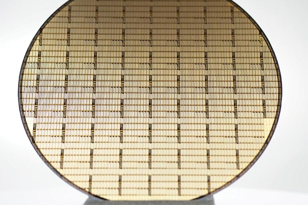
To speed up our reliability learning, we apply wafer-level test set-ups, with switching electronics fully integrated on the probe card. If we were to test in the classical way, using packaged parts, this would be slower and more cumbersome – before testing could commence, we would need to undertake a full back-end process and packaging. With our wafer-level approach, depending on the test, we can measure several thousand devices per day, rather than as few as possibly tens of devices per month (see Figure 6).
Another strength of our wafer-level DHTOL set-ups is that, thanks to their flexibility, they are well-suited to degradation model learning (see Figure 7). In the simplest way, we measure time-to-failure at 700 V, 650 V, and 600 V, and use the results to extrapolate the failure time for an application bias of 520 V.

Figure 7. Wafer-level switching DHTOL uses a sophisticated stressor
model based on a switching locus variation to extract the DHTOL lifetime
of processes and technologies.
We also employ a more advanced approach, tuning switching characteristics. They range from no overlap between the high voltage and the load current (so-called ‘soft switching’) to a large overlap between the two (‘hard switching’), and cover everything in between. This overlap, generating a high energy-loss in the device, acts as a key factor limiting end-of-life reliability. By drawing on this switching locus variation, and employing a new sophisticated stressor model, we are able to model the DHTOL lifetime of processes and technologies during development in GaN application-like conditions.
One of the most challenging tasks we face is generating the extrinsic model that’s used to estimate the infant mortality failure rate. In one case, we tested more than 100,000 parts in burn-in ovens at three different accelerated conditions to extract the voltage and temperature acceleration factors (see Figure 6).

Figure 8. Accelerated life stress testing is undertaken with an
extensive sample size, exceeding 100,000 devices, to identify both
intrinsic and extrinsic branches. The evaluation applies
well-established mathematical models that incorporate the mission
profile of the target application.
These figures are then applied to the application profile, to estimate the extrinsic branch and failure rates through the lifetime of the device (in the example shown (see Figure 8), 15 years lifetime is assured). Note that we have to use such a large statistical sample size, due to the extremely low extrinsic failure rates.
While such efforts are far from trivial, it’s crucial to understand the reliability of GaN. Without this, it’s not possible to unleash its full, tremendous potential.


