

Asymmetry spawns superior SiC superjunctions
By breaking conventional performance limits, asymmetric SiC superjunctions boost power-conversion efficiency.
BY DAISUKE IIZASA, HIROAKI SHIRAGA, SUGURU OKUYAMA, SEIGO MORI AND YUKI NAKANO FROM ROHM
Global electricity consumption is rocketing, driven by the growing adoption of electric vehicles and increasing demands on data centres. To increase supply, while addressing concerns related to carbon footprints, many nations are boosting their renewable energy systems. However, efforts in this direction should go hand-in-hand with increases in power-conversion efficiency, as every fraction of a percentage point ensures that the electrical energy that’s generated is used as wisely as possible.
Helping to succeed on this front is an uptake of SiC devices, now sitting at the heart of modernised electrical energy infrastructure. Thanks to their intrinsic material advantages, including a wide bandgap, a high critical electric field and excellent thermal conductivity, SiC devices operate efficiently, even when having to handle high voltages at high temperatures.

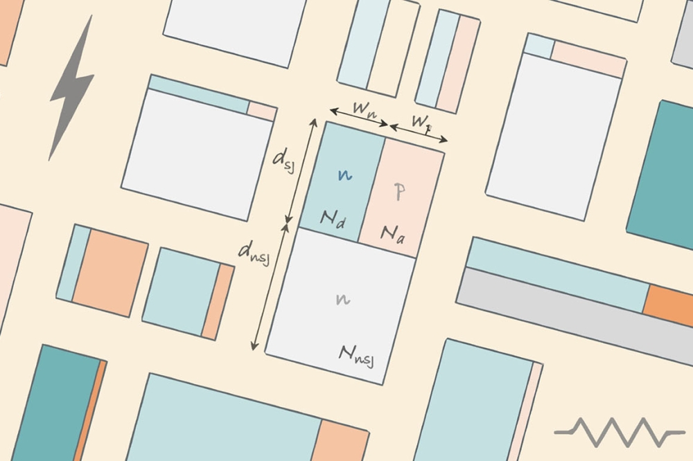
Figure 1. Cross-sections of SiC superjunction devices under reverse
bias. Panels (a) and (b) show full-superjunction structures with pillars
extending through the entire drift layer, while (c) illustrates a
semi-superjunction structure in which the pillars partially extend into
the drift layer above an additional drift region.
Within the diverse family of SiC device architectures, the superjunction structure attracts a great deal of attention. It is a promising approach to breaking the long-standing trade-off between specific on-resistance and breakdown voltage, a bottleneck that has traditionally constrained performance.
In the medium-voltage systems used in renewable-energy converters and electric-vehicle inverters, even modest reductions in specific on-resistance deliver meaningful gains in efficiency at the system level. But succeeding in this endeavour is not easy, as it is costly and slow to optimise SiC superjunction structures through experimental trial and error. The processing steps involved – such as trench-refill epitaxy, implantation into trench sidewalls, and repeated cycles of epitaxial growth and ion implantation – are demanding and highly sensitive to fabrication variability. Due to these challenges, theoretical evaluation is indispensable. When one works with a reliable computational model, this accelerates design cycles and clarifies the underlying physical limits, thereby providing a strong foundation for more-efficient, cost-effective manufacturing.
Initially, the superjunction concept took the form of a full-superjunction, with n-type and p-type pillars extending through the entire drift layer (see Figure 1 (a), (b)). Modifications have followed, such as semi-superjunctions that feature an additional drift region beneath the pillars (see Figure 1 (c)).

Figure 2. Impact ionisation anisotropy and breakdown paths in SiC superjunctions. (a) Electron impact ionisation is much stronger along the a-axis than the c-axis, highlighting the importance of crystal anisotropy. (b) Strong electric-field concentrations appear near pillar centres and interfaces, and the breakdown path typically follows these high-field regions.
The design space of full-superjunctions has been thoroughly explored, with investigations considering pillar doping, pillar width, and the depth of the superjunction region. Their fabrication is challenging, involving extremely intricate processes that include multiple high-energy implantation steps, combined with epitaxial growth or the use of trench-refill epitaxy.
In comparison, semi-superjunctions are more practical for real devices. However, despite this, there are relatively few theoretical studies of these structures, an omission that we are addressing at Rohm. Our investigation led to the design of asymmetric SiC superjunctions that can overcome conventional performance limits.
A particularly important, but often overlooked factor in the study of SiC superjunctions is impact ionisation anisotropy. Despite its strong influence on the breakdown behaviour of the SiC superjunction, optimisation studies tend to treat impact ionisation as isotropic – that’s a troublesome oversight that leaves a significant gap between theory and the real physics governing device performance. It is critical to capture anisotropy accurately, and this is needed to ensure a realistic prediction of blocking voltages and identification of the true performance limits of superjunction devices, especially when efforts are directed at balancing the specific on-resistance and blocking voltage.

Figure 3. Enhanced performance of semi-superjunctions achieved through
asymmetrically tuned geometry. A proportion of 0.5 for the n-pillar
corresponds to the perfectly symmetric case, which defines the
conventional performance optimum. Asymmetric geometries with wider n-pillars and narrower p-pillars provide further reductions in specific on-resistance beyond this symmetric limit.
Impact ionisation anisotropy
In stark contrast to silicon, SiC exhibits pronounced crystal anisotropy in impact ionisation coefficients. This variation originates from its crystal structure, with the excitation energy required to generate additional conduction carriers varying markedly with crystallographic direction. As a result, electrons and holes experience different avalanche generation rates, depending on the axis of travel, for example between the [0001] and [11‹bar›20] directions. In fact, the electron impact ionisation coefficient along the a-axis is significantly larger than that along the c-axis (see Figure 2(a)). Due to this anisotropy, SiC devices enter avalanche breakdown earlier than predicted by conventional isotropic models.
Therefore, the anisotropy associated with impact ionisation must be carefully considered when evaluating device behaviour near the critical electric field.

Figure 4. Maximum specific on-resistance enhancement obtained with
asymmetric geometry across different voltage classes. All voltage
classes show a substantial improvement compared with conventionally
optimised symmetric semi-superjunctions, with the best case appearing at
an n-pillar proportion of 0.9.
With superjunctions, it is particularly important to account for anisotropy associated with impact ionisation. In these devices, alternating n- and p-type pillars form a distinct two-dimensional electric-field landscape. There is charge compensation between the pillars, resulting in lateral depletion, which produces large electric-field peaks at pillar interfaces. These peaks strongly interact with the anisotropic impact ionisation process, as shown in Figure 2 (b).
Under these conditions, there are a number of electrical breakdown trajectories. Paths may run through the centres of the n- or p-pillars, or follow a winding route along the pillar interface, where there is a highly concentrated local electric field. Among these variations, the winding path tends to trigger the earliest breakdown. This is driven by strong coupling between the intense electric field that’s oriented along the a-axis in SiC superjunctions, and the pronounced anisotropy of the impact ionisation coefficients.
When simulations or theoretical models neglect anisotropy, the price that’s often paid is an overestimate of the blocking voltage. This oversight arises because the actual ionisation rate along the interface path is notably higher than that assumed in isotropic models. One unwanted, dire consequence of optimisation studies that ignore anisotropy is that they draw misleading conclusions concerning the performance ceiling of SiC superjunction devices. To ensure meaningful design and optimisation, prior to fabrication, it is essential to accurately capture the interplay between anisotropic impact ionisation and the superjunction field structure.

Figure 5. Mechanism behind the reduced specific on-resistance in
asymmetric semi-superjunctions and its impact on breakdown. (a) Specific
on-resistance improves when the p-pillar doping density is increased and the n-pillar
doping density is decreased, with key contributing factors such as
doping, incomplete ionisation, mobility and pillar width plotted
relative to the symmetric case. (b) Despite these changes, the
electric-field concentration at the pillar interface remains essentially
unchanged over the n-pillar proportion, allowing the device to sustain its breakdown voltage while benefiting from lower specific on-resistance.
Beyond symmetry
Traditionally, theoretical and TCAD-based analyses of SiC superjunctions tend to assume symmetric geometries, namely equal pillar widths and matched doping concentrations. This approach offers mathematical simplicity, as with symmetry geometries, charge balance is straightforward to satisfy and analytical treatment is far more manageable. However, there is a disconnect between these simulations and real devices – the latter rarely maintain ideal symmetry, as fabrication processes introduce unavoidable variations in geometry and doping.
In practice, asymmetries influence both specific on-resistance and blocking voltage. For example, widening the n-type pillar may lower the resistance by enhancing conductance, but this can be accompanied by a disturbing of charge balance and a strengthening of the electric-field concentration near the top of the n-pillar centre. Unfortunately, this electric-field localisation may be amplified by differences in doping concentration between n- and p-type pillars.
Collectively, these effects determine actual device performance, so it’s essential for predictive models to incorporate them in a physically consistent manner. Although prior studies have investigated asymmetric semi-superjunction geometries in terms of the trade-off between specific on-resistance and blocking voltage, they have failed to offer systematic insight, including the role that’s played by impact ionisation anisotropy.
Previous work by our team took an initial step in closing this gap, by developing a theoretical model for symmetric semi-superjunctions. That particular approach, which explicitly considered impact ionisation anisotropy, provided clear insight into the performance limit of symmetric structures when accounting for impact ionisation anisotropy.
The weakness of our initial model is that symmetry represents just one special case. To accurately reflect real devices, it is indispensable to use a more general framework that’s capable of handling arbitrary asymmetry. By developing such a model, we reveal how deviations from perfect symmetry influence static performance characteristics, and we define the attainable trade-off between the specific on-resistance and the blocking voltage beyond the symmetric regime.
A unified framework
Key to our progress is the development of a unified computation framework that provides performance evaluation of SiC superjunctions with arbitrary geometric asymmetries. The cornerstone of this framework is the derivation of an exact solution to Poisson’s equation. This solution provides closed-form expressions for the electric-field distribution as a function of position, doping concentration, and pillar width. With this approach the electric field can subsequently be referenced, allowing us to quantify the blocking voltage without having to rely on CPU-intensive discretised numerical computation.
In parallel, we have constructed an analytical formula for specific on-resistance. This model takes into account incomplete ionisation of dopants, as well as a mobility degradation that depends on doping levels.
By combining these expressions, we are able to analyse the trade-off between specific on-resistance and blocking voltage across a broad design space in a matter of seconds, using just a standard CPU. In sharp contrast, TCAD simulations typically take hours.
Our unified model combines computational efficiency with clear physical insight. It reveals how geometric parameters and doping concentrations jointly shape the electric-field landscape, and it clarifies which factors govern breakdown and conduction. Thanks to these valuable attributes, our framework functions as a powerful tool for pre-fabrication design optimisation, allowing rapid exploration of potential device structures and providing meaningful theoretical guidance for process engineers.
The asymmetric advantage
Using our unified computation model, we have systematically investigated how geometric asymmetry influences the relationship between specific on-resistance and blocking voltage. Our results reveal that well-designed asymmetric semi-superjunctions exceed the performance of symmetric ones, and effectively surpass the conventional design limit.
Highlighting this trend is a comparison of symmetric and asymmetric geometries that sustain a breakdown voltage of 3.2 kV, and have a 6 µm pillar pitch (see Figure 3). In this case, we have plotted the optimised specific on-resistance as a function of n-pillar proportion, which we define as the n-pillar width divided by the total pillar width. We keep the overall device pitch unchanged. The plot for 0.5 considers the perfectly symmetric case, which represents the theoretical optimum for symmetric semi-superjunctions. This graph also shows that widening the n-pillar while narrowing the p-pillar leads to a reduction in specific on-resistance, realised without compromising blocking voltage. The benefit is not trivial – it’s up to 16 percent lower than the symmetric optimum. The greatest gains are realised when the p-pillar is extremely narrow, corresponding to an n-pillar proportion of 0.9.
We have extended this analysis to several voltage classes (see Figure 4 for a summary of the results). For every voltage class, we have plotted the maximum reduction in specific on-resistance under an asymmetric geometry. The optimum gain always occurs at an n-pillar proportion of 0.9. We have found meaningful improvements in specific on-resistance for a wide range of voltage classes when adopting finely tuned asymmetric geometries. Enhancement is highest for 2.2 kV devices, which benefit from a 19 percent reduction in specific on-resistance.
To understand the origin of these improvements, we began by examining the design parameters that led to them. This included an investigation of how device performance evolves when geometry deviates from symmetry. Considering a 3.2 kV case, and the n-pillar proportion becoming larger, we have found that performance improves when the p-pillar doping density increases and the n-pillar doping density decreases. This shift in doping is needed to maintain charge balance under the wider n-pillar and narrower p-pillar configuration.
We are able to interpret the underlying physics of this state of affairs. When the n-pillar is wider, this boosts conductance by increasing the cross-sectional area for carriers, which reduces the specific on-resistance (see the lower panel of Figure 5 (a)). Meanwhile, when there’s a lowering of n-pillar doping, while raising the p-pillar doping to preserve charge balance, this suppresses incomplete ionisation and increases the carrier density at room temperature. Note that this adjustment also enhances electron mobility, further contributing to the reduction in specific on-resistance. These positive effects are considerable – they collectively outweighing the resistance increase normally associated with reducing the n-pillar doping density, and they enable an overall improvement in specific on-resistance for asymmetric geometries.
Another benefit of the optimised design is that it stabilises the electric-field profile in the superjunction region. Our work shows that the dominant contributor to electrical breakdown in optimised semi-superjunctions is the electric-field concentration at the p-n pillar interface (see Figure 5 (b)). According to our calculations, the electric-field components along the a-axis and c-axis of SiC, as well as the total field magnitude, remain essentially unchanged over the range of n-pillar proportions. This is a welcome finding, indicating that the blocking voltage remains stable, even in highly asymmetric geometries.
We can conclude that the resulting device configuration maintains a high breakdown voltage that’s comparable to symmetric designs while offering a significantly lower specific on-resistance. This finding highlights that geometry is a powerful design variable, which can be employed to enhance the performance of SiC superjunctions under impact ionisation anisotropy, supported by an efficient computation framework.
Looking ahead, we are expecting this combination of anisotropy-aware modelling and asymmetric design to have a significant impact on the future of SiC superjunctions, informing both discrete device roadmaps and volume-production design rules. When manufacturers embed this framework early in the development flow, they will shorten iteration cycles, reduce process risk, and have the opportunity to explore higher-voltage operating regimes that would be prohibitively expensive to probe by just trial and error.
•This work is based on results obtained from a Project, JPNP21014, subsidized by the New Energy and Industrial Technology Development Organization (NEDO).


