
Unlocking the potential of AlN-buffer HEMTs
Reducing current collapse and boosting blocking voltage enables a doubling of the continuous-wave output power of AlN-buffer HEMTs.
Engineers from Soctera and Trinix Technology are claiming to have delivered a substantial increase in the continuous-wave (CW) output power of AlN-buffer HEMTs.
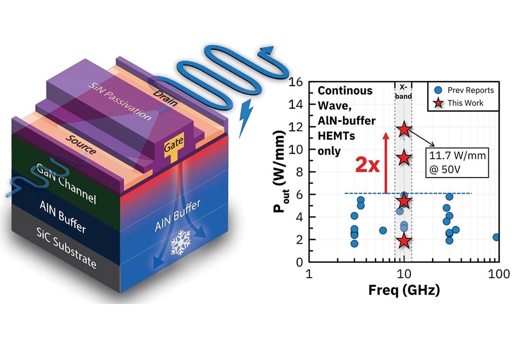
According to team spokesman, Soctera CTO Reet Chaudhuri, prior to this success, CW output powers of AlN-buffer HEMTs have been below 6 W mm-1, leading to scepticism surrounding this promising technology. While there is much reason for optimism, due to the excellent thermal conductivity of AlN, underwhelming output powers have led to concerns surrounding the two-dimensional hole gas and traps at the interface between GaN and AlN.
“We show that 6 W mm-1 is not an intrinsic limit, demonstrating record high output powers of more than 11 W mm-1 for AlN-buffer HEMTs across the frequency spectrum,” says Chaudhuri.
Previous generations of AlN-buffer HEMTs have been held back by current collapse and/or breakdown. Amongst efforts to improve performance, work has been directed at reducing dispersion, with approaches including the introduction of a δ-doped back barrier. However, successes have tended to come with a trade-off in breakdown voltage.
Chaudhuri and co-workers argue that they are breaking new ground by reducing current collapse while simultaneously increasing breakdown voltage, likely through a reduction in surface traps. “These combined factors enable us to access CW output powers higher than previously reported in AlN-buffer HEMTs.”
Fabrication of this class of transistor began by loading 100 mm semi-insulating SiC substrates into an MOCVD chamber and depositing metal-polar heterostructures. The epi-stack consists of an AlN buffer layer, and undoped GaN channel, and an AlGaN barrier.

Soctera’s AlN-buffer HEMTs deliver a ground-breaking CS output power density, attributed to an advanced fabrication flow.
To determine the thermal resistance from the two-dimensional electron gas (2DEG) channel to the SiC substrate, the team turned to frequency-domain and steady-state transient reflectometry. This revealed a thermal resistance of 5.5 m2 K GW-1, around one third of that for a standard HEMT featuring a 1.5 µm-thick GaN buffer on a SiC substrate.
According to room-temperature Hall effect measurements on the AlN-buffer heterostructure, the 2DEG has a density of around 1 x 1013 cm-2 and a mobility of around 1700 cm2 V-1 s-1.
Using these epiwafers, Chaudhuri and co-workers formed two-fingered HEMTs featuring SiN passivation, a source-to-drain distance of 2 µm, and a gate width of 2 x 100 µm.
Measurements on these devices determined a breakdown voltage of 98 V, and a peak CW output power of 11.7 W mm-1 at a drain-source voltage of 50 V. Maximum output power exhibits an almost linear increase with operating bias.
Benchmarking the maximum CW output power against other AlN-buffer HEMTs has shown that the team’s transistors produce the highest output power across the entire frequency spectrum, and deliver a power almost double that of the previous record.
Chaudhuri says that Soctera is actively commercialising its technology, which will bring electrically and thermally co-optimised GaN power amplifiers (PAs) to market. “These PAs are specifically designed for next-generation communication networks, offering significant size, weight, power, and cost benefits, and reduced reliance on foreign supply.”
Developed in partnership with a US-based supply chain, Soctera’s initial ‘samplable’ PAs are scheduled for launch by the end of this year.
The company will continue to develop its device technology. Efforts will now be directed at utilising source-connected field plates to enhance breakdown voltage and power handling capabilities, while simultaneously optimising device design for maximum thermal performance.
“On the manufacturing side, we are concentrating on scaling-up production, maximising yield, and ensuring high uniformity across the wafer, as we move closer to high-volume production,” reveals Chaudhuri.
Reference R. Chaudhuri et al. IEEE Electron. Dev. Lett. 47 680 (2026)


