
Bosch launches 3rd generation SiC MOSFETs
Bosch has announced its 3rd generation SiC MOSFETs, based on the company's dual-channel trench SiC architecture with lower on-resistance, better ruggedness, and smaller chip sizes for broader EV adoption.
A 20 percent reduction in specific on-resistance, around 10 percent higher short-circuit withstand capability, and a 40 percent thinner die enable clear efficiency gains and more cost-effective power module designs, according to the company.
At the same time, the reduced die size has a direct impact on production efficiency and system-level costs, further supported by the transition to 200 mm wafer manufacturing, which increases chip output per wafer.
While Bosch’s SiC chips are well-established in the demanding environment of high-performance electric vehicles, yhe company says these new features change the economic equation around SiC chip uses, enabling compact, efficient inverter and power module designs across a wider range of EVs from premium sports cars to mass-market models.
Gen 3 SiC MOSFETs offer measurable improvements in three key areas for automotive applications: electrical performance, thermal performance, and ruggedness.
In terms of thermal performance, reducing die thickness by 40 percent directly enhances heat dissipation and thermal conductivity. This supports higher power density and more efficient thermal management in high-performance semiconductor systems.
For ruggedness, the short-circuit withstand capability increases by about 10 percent, supported by the optimised two-zone JFET region and enhanced gate oxide design. The design also improves robustness against parasitic turn-on at high switching speeds.
Additionally, the intrinsic body diode is optimised for soft recovery behaviour across the full automotive temperature range of -40°C to 200°C, reducing electrical stress during switching events and supporting stable operation under demanding conditions.
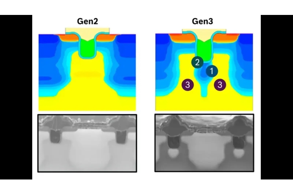
Three specific advancements in Gen 3 SiC-MOSFET architecture are shown in the diagram above including the trench (green), the new shield implant below the trench (blue), and the two-zone JFET region (yellow).
First, additional p-type shielding region introduced directly below the trench, provides full protection against off-state electric fields. This contributes to improved long-term gate oxide reliability under typical operating conditions. The existing hard mask of the trench etching process was reused for the new trench shield implant, eliminating the need for an additional lithographic process step.
Second, two-zone structure in the JFET region beneath the trench is such that each channel now corresponds to its own JFET region, providing significantly finer control over electric field distribution during both normal operation and fault events. This improves the critical trade-off between on-resistance (RonA) and short-circuit withstand time (SCWT), expanding the available design space for robust, high-performance SiC power semiconductors.
Third, the die thickness in Gen 3 is reduced by 40 percent to only 100 µm. This reduces material usage and places the active semiconductor layer closer to the heat sink, accelerating heat dissipation.
Anne Bedacht, head of product management for power semiconductors at Bosch commented: "The Gen 3 upgrades are noteworthy for two reasons: their combined effect and how our engineers integrated them into well-established production processes. Our design-for-manufacturability approach ensures that Gen 3 is production-ready and cost-effective from the outset."


