
Propelling the PCSEL into the deep-UV
With edge-emitters and VCSELs stalling, is the PCSEL emerging as the best candidate for delivering laser emission deep into the UV?
BY DOĞUKAN APAYDIN FROM CHALMERS UNIVERSITY OF TECHNOLOGY
Since the birth of the semiconductor laser in the early 1960s, effort has been directed at expanding its spectral range. Much progress has been made at ever longer wavelengths, with success stemming from the introduction of a new architecture, the quantum cascade laser. In contrast, stretching to shorter wavelengths has been far less productive, with the greatest progress over the last few decades involving the introduction of a new material system: GaN and its related alloys, particularly AlGaN. However, while these nitrides undoubtedly offer the best chance of success, maybe they need to be combined with an alternative design, so they can excel when plunging deep into the depths of the UV?

Figure 1. Emission wavelengths of III-nitride PCSELs that have been demonstrated by various groups over the years.
The AlGaN challenge
The III-N family spans the visible to the UV, with shorter wavelengths reached by increasing the aluminium content of AlGaN. All optoelectronic devices made from this material share weaknesses, including a high defect density, low electrical and thermal conductivity, low refractive index contrast and low material gain.
As these issues are yet to been fully solved, despite growing demand for diode lasers throughout the UV, many applications are relying on excimer lasers and frequency-converted solid-state lasers, sources that are far from ideal, being large, expensive and not power efficient. As semiconductor lasers are small, compact and low-cost, if they could perform in the UV, they would be compelling candidates for spectroscopy, lithography and biomedical imaging – and possibly a number of new applications. However, today’s devices emitting in the UV fall far short of the performance of their visible cousins, and closing this gap is challenging.
But there are glimmers of hope. In late 2022, a collaboration between Hiroshi Amano’s team at Nagoya University and the AlN substrate producer Asahi Kasei Corporation reported room-temperature, continuous-wave lasing at 274 nm from an edge-emitting laser grown on a bulk AlN substrate. Key to this success is combatting low p-type conductivity with a distributed polarisation-doped layer featuring a gradual change in material composition. Unlike impurity doping, which yields very low hole concentrations at room temperature, due to the high activation energy of magnesium, distributed polarisation doping reaches higher hole concentrations. By introducing distributed polarisation-doping, it is possible to produce current-injection deep-UV lasers. Building on this success, Ultec, a spin-out of this Japanese startup, introduced the first commercial deep-UV laser diode.

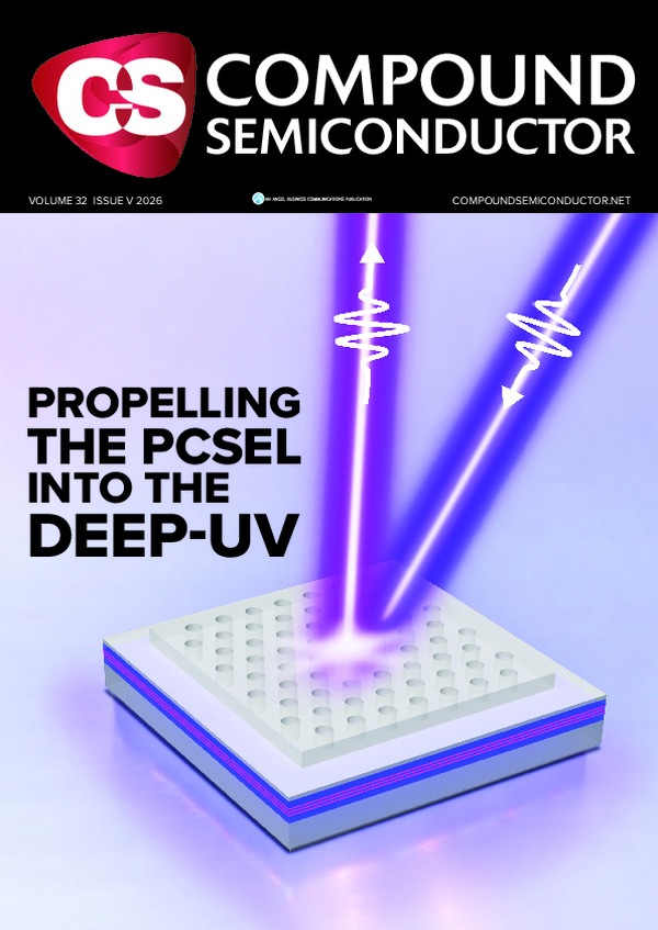
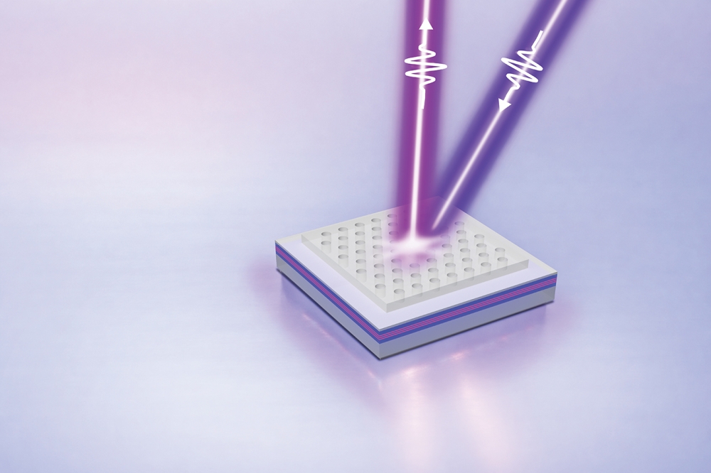
Figure 2. Illustration of the pump beam and the surface emission in a
deep-UV PCSEL, with insets showing a topview SEM of the hexagonal
photonic-crystal pattern and the AlGaN epitaxial stack.
Other noteworthy successes include great progress in the UVB, where, very recently, Meijo University demonstrated the first continuous-wave lasing. And in just the last month or so, Zetian Mi’s team from the University of Michigan announced a 299 nm laser produced by MBE. Driven in pulsed mode, this device has a very low threshold current density.
Within the nitride community, efforts have also been directed at VCSELs, which have a number of merits over edge-emitters, including being better suited to high-volume manufacture. However, it is far harder to make a VCSEL from AlGaN than AlGaAs. All VCSELs feature a pair of highly reflective mirrors made from distributed Bragg reflectors. With a GaAs VCSEL, the pairing of GaAs and AlAs is well suited to this task – but there’s no good equivalent for the nitrides, due to a lack of candidates that combine an adequate refractive index contrast with lattice matching. Turning to dielectric mirrors addresses this issue, but demands substrate removal, and that’s not easy to do. Note that to date, in the UV, lasing has only been demonstrated under pulsed optical pumping.

Figure 3. Measured PCSEL far-field emission patterns for filling factors
of 10 percent (left), 15 percent (center) and 22 percent (right);
angular range ± 20 °.
PCSELs: A potential solution
While the performance of edge-emitters and VCSELs has not plateaued, of all the approaches for a III-N UV source, the photonic crystal surface-emitting laser (PCSEL) has the greatest promise. This class of laser employs a two-dimensional (2D) photonic crystal for in-plane optical feedback. What makes it particularly compelling is its large gain area, enabling high output powers to be combined with single-mode operation. Devices deliver a circularly symmetric beam with a low divergence angle, usually less than 1 °.
The inventor of the PCSEL is Susumu Noda from Kyoto University, Japan. In 1999, along with his co-workers, he demonstrated the first PCSEL at infrared wavelengths. Since then, Noda’s team have made significant strides, including, in 2008, GaN-based PCSELs delivering blue lasing with current injection. This group has also demonstrated the first green PCSEL, and a PCSEL producing an output of hundreds of watts.
Where Noda has led, a growing number are following. There have now been demonstrations by several groups of PCSELs based on the III-nitride material system emitting in the blue (see Figure 1).
For PCSELs operating at visible wavelengths, performance is now starting to catch up with their infrared counterparts. However, in the UV, the pace has been much slower.

Figure 4. Measured PCSEL band structures for filling factors of 10
percent (left), 15 percent (center), and 22 percent (right). The left
half of each figure shows the below threshold band structure, the right
half shows the above threshold band structure.
First deep-UV PCSELs
To date, there has been a limited number of reports of lasing in the UV, with none reaching the deep-UV regime until recently.
Helping to drive the latest progress is our team from Chalmers University of Technology, Sweden. Our important milestone towards shorter wavelengths has been the demonstration of the first deep-UV PCSELs under pulsed optical pumping at room temperature. Thanks to this, PCSELs now cover a larger region of this domain.
Growth of our AlGaN epitaxial stack on a sapphire substrate has been undertaken by our collaborators at the Technical University of Berlin (see Figure 2). They have provided us with material with an estimated defect density of 5 x 108 cm-2 – much higher than that for GaAs-based devices, which have defect densities typically ranging from 104 cm-2 to 106 cm-2.
Device fabrication began by spinning a high-resolution negative electron-beam resist, HSQ, on the epiwafers, prior to electron-beam exposure and development. When exposed or annealed, HSQ turns into SiOx, creating a hard mask for etching. But that’s not all – this oxide helps avoid imperfections introduced by pattern-transfer methods, such as lift-off. That’s highly valued when producing devices for the deep-UV, because feature size scales with wavelength. After exposure, we directly transfer 140-µm-wide photonic crystals with a lattice constant of 140 nm into the top AlN cladding, using Cl₂/Ar dry etching. A buffered oxide etchant removes the remaining resist.
Most producers of PCSELs encapsulate the photonic crystal in a subsequent regrowth step. We take a different approach, bringing both benefits and trade-offs. Our regrowth-free approach simplifies the fabrication process, which is expensive and time consuming, but poses the risk of introducing plasma-induced damage to the quantum wells, due to deeper photonic crystal etching.
One of the key requirements for the PCSEL is that the optical mode in the waveguide has sufficient confinement from the photonic crystal to be modulated by the periodicity. This is accomplished by ensuring that the photonic crystal is sufficiently close to the quantum wells. If we fail on that front with an etch that’s too shallow, the lasing threshold is then too high, due to insufficient confinement. But go too far the other way, with an etch that’s too aggressive or too close to the quantum wells, and then there’s the threat of degraded quantum wells, increasing threshold, and in the worst case, preventing the device from lasing.

Figure 5. Angleresolved photoluminescence setup used for deep-UV PCSEL characterisation, with illustrations of the 266 nm pump beam and the PCSEL emission.
By going regrowth-free, we are adopting an approach that’s applied to existing edge-emitting laser structures that are proven to lase under current injection. In terms of epitaxial structure and fabrication, our regrowth-free PCSELs are not that different to edge-emitting lasers, with a waveguide between two claddings and a photonic crystal. What this means is that it should be possible to easily integrate a 2D photonic crystal and realise electrically-driven PCSELs in the deep-UV.
When pumping our PCSELs with a 266 nm laser that provides 0.55 ns pulses at a 20 kHz repetition rate, they exhibit a single lasing peak around 279 nm. Initial demonstrations produce lasing thresholds of around 17 MW cm-2 at room temperature, so significantly higher than optically pumped deep-UV edge-emitting lasers, which have values generally around 1 MW cm-2 at similar wavelengths. But that gap is closing, with our most recent devices having thresholds around 5 MW cm-2, thanks to optimised photonic-crystal fabrication. Note that the pump beam is absorbed only by the quantum wells.
Strengthening 2D coupling
Unlike a distributed feedback laser, a PCSEL does not couple light in just one direction. Instead, it is coupled in 2D, essentially leading to a 2D standing wave. However, it’s not easy to realise sufficient 2D coupling in a square lattice with circular holes, because the wavevector must change direction by 90 °. If the 2D coupling is weak, oscillation tends to occur mostly in 1D, causing the 2D photonic crystal to act as a 1D grating. In this case, a highly divergent beam results.
This undesirable emission profile is a particular concern in aluminium-rich III-nitride materials. For these PCSELs, the low refractive-index contrast reduces the in-plane coupling strength. Another issue is that the short wavelength, and therefore the small feature size, makes the device more sensitive to surface roughness and fabrication imperfections. Taken together, these drawbacks make it particularly challenging to realise robust 2D operation.
Moving to a hexagonal lattice is a solution. As 2D coupling occurs at 60 ° and 120 °, it is easier to obtain sufficient 2D coupling strength with a hexagonal lattice. We have pursued this design, using a hexagonal lattice with circular holes. This architecture has helped increase symmetry and decrease the threshold.
If a PCSEL with circular holes were to have an infinite photonic crystal, there would be no surface emission, since the fields are perfectly symmetric and the modes are symmetry-protected. But real photonic crystals have a finite size. Thanks to this, the electric field is perturbed by the edge of the photonic crystal and symmetry is broken, enabling vertical outcoupling.
However, as the device size increases, wall-plug efficiency falls. This occurs because the rate of increase in the device area exceeds the rate of increase in the area that light can outcouple. One option for overcoming this problem, and enhancing outcoupling, is to introduce asymmetric hole shapes that intentionally break the symmetry and enhance vertical outcoupling. More recently, some groups have adopted a double-lattice square lattice, an architecture that increases modal discrimination while maintaining sufficient 2D coupling strength.
This has enabled high-power single-mode operation in the infrared and blue. However, transferring this approach to the deep-UV is challenging, because a single-lattice square has a smaller lattice constant than a hexagonal lattice for the same operation wavelength – for example, 138 nm for a hexagonal lattice, and 119.5 nm for a square lattice – and it’s far from easy to fit a double hole in the unit cell.
Ensuring low divergence
For PCSELs, an important design parameter is the size of the air holes. This is often defined as the filling factor: the ratio of the air hole area to the unit cell area.
For small filling factors, such as 10 percent or so and associated with small hole sizes, the 2D coupling strength is weak and 1D oscillations dominate emission. This leads to highly divergent far-field emission patterns, extending up to 20 ° (see Figure 3).
Increasing the filling factor to 15 percent boosts the 2D coupling strength, and delivers benefits associated with the 2D periodicity of the photonic crystal. This fill factor leads to a donut-shaped emission pattern with a low divergence angle.
Going to even larger filling factors of around 20 percent or more ensures high 2D coupling. However, this also results in a peculiar divergent emission pattern that is an exact copy of the cross-section of the band structure at the lasing wavelength. As filling factors increase, they cause the device to lase at a different bandedge mode. In our band structure measurements, we have observed these changes in the lasing band edge mode (see Figure 4). This has led us to conclude that selecting the optimal filling factor is extremely important in deep-UV PCSELs.
Next: current injection
Current injection is always the ultimate goal for any semiconductor laser. We are working towards this, having shown that the PCSEL concept can be extended into the deep-UV using aluminium-rich III-nitrides, despite their low refractive index contrast and the small feature sizes required at these wavelengths. As technology matures, we expect deep-UV PCSELs to operate under current injection, just like their infrared and visible counterparts. However, success will require addressing several questions, including how to spread the current efficiently across a large photonic crystal area.
With our PCSELs, while the epitaxial layers are similar to those of an edge-emitting laser, the current spreading requirements are very different. In edge-emitters, the current only has to be spread over a lateral distance of the order of the ridge width; but in PCSELs, this distance can range from a few tens of micrometres to millimetres. For blue and infrared PCSELs, one option is to use conductive substrates to aid lateral spreading. Unfortunately, that’s not possible with deep-UV PCSELs, due to the lack of conductive substrates. One solution is substrate removal, but that does not guarantee current uniformity, which could impact lasing performance, for example, by promoting higher-order modes or preventing the formation of a 2D standing field.
Solving these issues will be challenging, but the path is clear. There’s good reason to believe that thanks to progress in materials and photonic crystal design, it will not be long before we have the first electrically driven deep-UV PCSEL.


